#Xilinx Vivado
Text
youtube
VHDL Tutorial : Your First VHDL Design: VHDL Entity & Architecture - A Beginner's Guide
Welcome to the ultimate beginner's guide for Your First VHDL Design! In this video, we will dive into the fundamentals of VHDL Entity and Architecture and provide you with a comprehensive understanding of the topic. Whether you are new to VHDL or looking to refresh your knowledge, this guide is designed to help you get started and pave your way to becoming an expert VHDL designer. In this tutorial, we will cover the basics of VHDL, starting with the VHDL Entity and its crucial role in the design process. You will learn how to define and describe the inputs and outputs of your VHDL design using the Entity section, providing the necessary specifications for your project. Moving on, we will explore the VHDL Architecture, which defines the actual implementation of your design. Through a step-by-step walkthrough, you will discover how to construct the architecture block by block, ensuring a well-structured and functional VHDL design. To make the learning experience more practical, we will dive into real-world examples and demonstrate each concept using a popular VHDL software tool. You'll witness the transition from theory to practice, gaining hands-on experience in VHDL design. With this beginner's guide, you'll not only grasp the essentials of VHDL Entity and Architecture but also acquire the ability to kickstart your own VHDL designs, opening up a wide range of possibilities in digital circuit design. Subscribe to our channel for more exciting VHDL tutorials and stay tuned for upcoming videos in this series where we will explore advanced VHDL concepts and applications.
Subscribe to "Learn And Grow Community"
YouTube : https://www.youtube.com/@LearnAndGrowCommunity
LinkedIn Group : https://www.linkedin.com/groups/7478922/
Blog : https://LearnAndGrowCommunity.blogspot.com/
Facebook : https://www.facebook.com/JoinLearnAndGrowCommunity/
Twitter Handle : https://twitter.com/LNG_Community
DailyMotion : https://www.dailymotion.com/LearnAndGrowCommunity
Instagram Handle : https://www.instagram.com/LearnAndGrowCommunity/
Follow #LearnAndGrowCommunity
#VHDL#VHDL Entity#VHDL Architecture#VHDL Design#Beginner's Guide#Digital Circuit Design#VHDL Tutorial#VHDL Basics#VHDL Examples#VHDL Software#Learn VHDL#VHDL Learning#VHDL Step-by-step#VHDL Introduction#VHDL Fundamentals#VHDL Engineering#Hardware Design#Circuit Design#Xilinx ISE#Xilinx Vivado#Digital#ASIC#Engineering#Students#Training#Tutorial#Altera#Hardware description language#modeling style#data flow
1 note
·
View note
Text
CMSIS support in IDesignSpec
IDesignSpecTM (IDS) is a product suite that improves the productivity of FPGA/ASIC, IP/SoC, and System Development teams. These products encompass an innovative register information management system to capture hardware functional specifications and addressable register specifications in a single "executable" specification. All downstream code and documentation for the addressable registers, sequences or interrupts can be generated from a single specification along with CMSIS support.
CMSIS is a standard developed by ARM for Cortex-M processors. CMSIS allows compatible device support and provides software interfaces to the microprocessor and its peripherals so that software can be reused. CMSIS also helps to reduce the time to market for newly manufactured devices.
The following problems can be solved by IDS when it generates CMSIS output:
Automatic generation of CMSIS-SVD files for Silicon vendors. They don’t need to write it.
Silicon vendors can give these files to Tool vendors.
SVD files are used for debugging purposes for programmers.
IDS supports ARM-provided CMSIS-SVD component of CMSIS as an output, CMSIS stands for Common Microcontroller Software Interface Standard. The CMSIS System View Description format(CMSIS-SVD) standardizes the description of the system which is developed with Arm Cortex-M processor-based microcontrollers, in particular, the memory-mapped registers of peripherals.

Silicon vendors require a CMSIS-SVD file with a .svd extension which will further aid in the real-time debugging of programmer’s software code. Based on this file, the silicon vendor will further develop the startup code and the system initialization files specific to their device. Before CMSIS support, programmers could see only data inside the peripheral registers connected with microprocessors inside microcontrollers. But with CMSIS-SVD support custom peripheral registers data can also be seen.
IDS generated XML format SVD file has Device hierarchy acceptable by Keil (ARM-supported tool)with zero errors i.e. device-cpu-peripherals-peripheral-registers-register-fields. We provide the device’s peripherals base address( which is selected by the location of the executable memory of the microcontroller) and offset of Registers and access type etc. ARM Command Utility (SVDConv.exe) converts the SVD file into a Special Function Register(SFR) file which is shown below in the snippet.
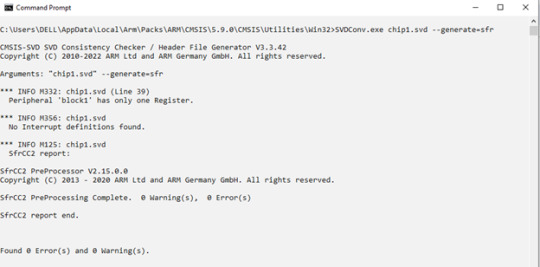
Custom peripheral registers can also be seen for debugging purposes from the SFR file which has to be added in the Keil with the respective path in the “option in target dialog” section which is shown below in the snippet.

Figure 3: SFR file in Keil µvision-An ARM Tool
Validation of data written or read inside Peripheral Registers, connected with ARM processor, is possible through FPGA boards like Zedboard with the help of Xilinx Vivado-SDK platform. Now It is possible in the ARM's tool Keil itself. Keil supports XML format.
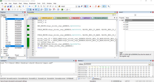
In IDS-Validate a programmer can give inputs such as Register specs and sequence specifications. The tool will generate output as a Header file, SVD (XML) file, and sequence APIs or firmware. With the help of these outputs, programs can be executed in Keil, as shown below in the block diagram.
Figure 4: Block Diagram of IDS Role play with Keil µvision
In IDS-Validate, Programmers generate their firmware which is used to perform operations on custom peripheral devices and see the results. If results are not coming correctly then programmers can open the debug window. Keil opens a System Viewer, a sub-menu of the Peripherals menu in the toolbar, in which a device’s registers can be seen., The programmer can execute the program step by step and data can be validated inside peripheral registers which are shown below in the snippet.
On the Right side of the snippet, a window is opened which is called a system viewer. Inside this window peripheral “block1” and register “reg1” and fields “f1,f2,f3,f4” appear clear and data can be seen inside Register and their fields.
Conclusion
IDS is a powerful tool that generates SVD file, Firmware, and Device header file, Programmers just need to install Keil and run the firmware with a custom SVD file. Firmware can be the programmer's own programs or IDS-generated sequences. No need for another tool debugger.
Silicon vendors don't need to write SVD files who use the IDS tool to generate IPs. They can use IDS-generated SVD files to give tool vendors for programming purposes. If they change Specs CMSIS-SVD file automatically will be changed. The SVD file works well with the ARM processor and in the Keil environment, any customer who needs to create an ARM-supported SVD file can rely on our tool.
Call to action
To get more information about how we can help you to create an ARM-supported System View Description file reach out here.
0 notes
Text
Digilent Basys 3 Artix-7 FPGA Trainer Board: Recommended for Introductory Users.

Designed for students and beginners looking to understand Digital Logic, fundamentals of FPGAs
Features the Xilinx Artix 7 FPGA compatible with Vivado Design Suite WebPACK Edition (free download available from Xilinx)
On board user interfaces include 16 user switches, 16 LEDs, 5 user pushbuttons, and a
Expansion opportunities with four Pmod ports including 3 standard 12-pin Pmod ports and 1 dual
Does NOT ship with micro USB cable
#Digilent Basys 3 Artix-7#fpgatrainerboard#affiliate marketing#digital marketing#internet marketing#online marketing#youtube
0 notes
Text
VHDL VS VERILOG
The comments all include links to other websites or publications. Let me first create the answer story. After reading this response, one should clearly understand Verilog HDL and where they stand in the learning process.
Verilog is not a programming language. It isn't used in any platform for development reasons, and it doesn't make programming easier (relating to scripting). It does not create an environment or user interface that is interesting.
Verilog coding builds a digital circuit for a behavioural purpose while simultaneously modelling it, resulting in digital circuits. Before moving on to Verilog, make sure the digital circuit is in your blood and not in your heart. It breaks and also fails!
How should you proceed with digital circuits? Start learning about the following topics: gates, flip-flops, shift registers, counters, adders, subtractors, multiplexers, demultiplexers, priority encoders, encoders, decoders, K-maps, boolean algebra, and De-law. Morgan's Is that all? Nope. state machines as well They form the nucleus of the design cycle.

Best references Digital Circuit :
Morris, M. digital design by Mano. You will find clear foundation in this text. You won't struggle to understand it here.
Digital Design Team at Wakerly (Pearson publication). You can acquire sophisticated digital design methods from this book.
CMOS VLSI Design by Neil Weste and David Harris Without missing a word, give the third chapter your undivided attention. maximise the depth of your comprehension. at the very least, the construction of hardware gates and flops.
Now that you've developed a digital circuit in your brain. You understand how nanoscale technology functions and how electrical impulses go from one spot to another in a finite amount of time (3rd reference in the digital circuit). Let's go on to a thorough examination of Verilog.
Best References Verilog HDL :
Verilog by Samir Palnitkar. Beginners can easily understand this text. You don't dream about actual use. It can be used to create the necessary codes for logic circuits (synthesize-able). citations for digital design Examine it to see what you are able to write.
Award-Winning Verilog & System by Cliff Cummings Papers on Verilog is a source that is cited. Consider the following quotation to be holy Verilog. Read Verilog's documentation slowly. It's gratuitous. Use this reference if you are familiar with the words timing, power, and optimization in digital circuits.
Not all codes will result in digital circuits that can be used practically. You must be familiar with each keyword's usage. In Verilog, some keywords are created solely for simulation purposes; they don't produce any logic circuits.
Never, ever attempt Discover something new on Asicworld.com. Use it only for syntax.
Never, ever, ever believe any code you find online. It's terrible. You'll understand it afterwards. It prevents anyone from growing as a result.
Having trouble learning some subjects? Try to use prominent university names in the search field. comparable to "Stanford studies digital design." Materials are created by researchers and clever people worldwide. It will enchant you.
Try to familiarise yourself with tools like ModelSim, Xilinx Vivado, and Microsemi Libero. Everyone has been set free. I wholeheartedly support Vivado.
Some suggestions suggest reading up on static timing analysis, critical pathways, and data paths. That, however, is not a part of Verilog HDL. They are all engaged in the creation of semiconductors, which uses analysis tools.
robust typing is a VHDL term. Beginners will find it more challenging to make mistakes because the compiler will stop you from creating bad code. In Verilog, weak typing is employed. You can write shorter, but inaccurate, code thanks to it.
Verilog is more like a programming language than C. Because of this, someone who is knowledgeable in C will have an easier time reading and understanding Verilog's operations.
Using VHDL involves a lot of typing. For the same task, Verilog often utilises less code.
VHDL is very deterministic, in contrast to Verilog, which can occasionally be non-deterministic.
None of these, however, are more significant than the others. You should learn Verilog or VHDL depending on which one you are more likely to use at business or in education.
If your university uses Verilog, great! If nearby companies that you might wish to work for use VHDL, learn it! The people who use VHDL and Verilog depend greatly on where in the world you are. By entering VHDL vs. Verilog into Google Trends, you may start to receive a pretty clear indicator of which language you should be learning first.
The picture up above contains a lot of intriguing elements. The first is that VHDL and Verilog have both received about the same amount of queries on Google over the past year. This suggests that individuals who are interested in learning more about them find the two to be almost equally popular. I also saw a substantial reduction soon before Christmas, which is worthy of noting.and the New Year. I can only assume that people aren't searching for their HDL problems on Google during this time because they aren't at work or school.
In India and the US, where VHDL and Verilog appear to be almost equally popular, Google searches are most common. Verilog is slightly more popular than VHDL in the US. I am aware from personal experience that the US business sector favours Verilog whereas the defence sector typically favours VHDL. You'll observe that in Germany and France, VHDL is much more widely used than Verilog. If you are from either of these two countries, I would strongly recommend learning VHDL first! Establish your priorities because Verilog is unquestionably more popular than VHDL in China and South Korea.
Conclusion:
Verilog is an HDL used to model electronic systems, whereas VHDL is an HDL used in electronic design automation to specify digital and mixed-signal systems such as field programmable gate arrays and integrated circuits.
0 notes
Text
Lab 3: Single-Cycle CPU Solution
Lab 3: Single-Cycle CPU Solution
Goal
Based on Lab 2 (simple single-cycle CPU), add a memory unit to implement a complete single-cycle CPU which can run R-type, I-type and jump instructions.
Requirement
Please use Xilinx ISE or Vivado as your HDL simulator and note in your report.
Please attach your names and student IDs as comment at the top of each file.
Refer to Lab 2 for the top module’s name and I/O…

View On WordPress
0 notes
Text
Extending Single-Cycle MIPS Processor & Experiments on SystemVerilog and BASYS3 Board Solution
Extending Single-Cycle MIPS Processor & Experiments on SystemVerilog and BASYS3 Board Solution
Purpose: Extending MIPS-lite processor by adding new instructions to the datapath. Bringing new capabilities to the processor by adding new control signals, muxes etc. Simulating the extended processor both on software (Xilinx Vivado) and hardware (BASYS3 Board).
Summary
Part 1 (50 points): Examining the new instructions thoroughly and designing the changes that need to be made in the…

View On WordPress
0 notes
Text
SLX FPGA v2019.4 Delivers an Average of 45x HLS Performance Improvement
SLX FPGA v2019.4 Delivers an Average of 45x HLS Performance Improvement
Press Release
–
updated: Dec 16, 2019
SAN JOSE, Calif.,
December 16, 2019 (Newswire.com) –
Silexica (silexica.com) has announced the release of SLX FPGA v19.4, designed to help developers prepare and optimize C/C++ code for high-level synthesis (HLS) in Xilinx’s VivadoTM and VitisTM HLS design flows. SLX FPGA v19.4 provides performance improvements that deliver, on average, a 45x increase in…
View On WordPress
#Ai#Code analysis#embedded computing#FPGA#High-level Synthesis#HLS#Performance Optimization#Vivado#Xilinx
0 notes
Photo

Agimus Technologies Low Cost Xilinx FPGA Kits. Best Suited For Engineering, Diploma and ITI Syllabus. Supports Xilinx Vivado and ISE Software Tools. Apart from Xilinx FPGA Complete kits were designed and Developed in India Under #atmanirbharabhiyan #athmanirbharbharat #makeindia. Contact Agimus Technologies Pvt. Ltd for More Details. +91 9538757011 We Also under take FPGA Board Design Related Projects. #fpgadesign #fpga #hdl #vhdl #veriloghdl #verilog_programming #engineeringstudents #engineeringcolleges #diploma #iti #vivado #XilinxFPGA #xilinx #engineeringlaboratory #engineeringlabs #diplomalabs #fpgaproject #mtechprojects #beprojects #diplomaproject #vlsidesign #VLSI #spartanfpga #artixfpga #artix #xilinxiseatingourbrains #makeinindia (at Agimus Technologies PVT LTD) https://www.instagram.com/p/CDFnEHbHh83/?igshid=1d3vlz6ytqk7u
#atmanirbharabhiyan#athmanirbharbharat#makeindia#fpgadesign#fpga#hdl#vhdl#veriloghdl#verilog_programming#engineeringstudents#engineeringcolleges#diploma#iti#vivado#xilinxfpga#xilinx#engineeringlaboratory#engineeringlabs#diplomalabs#fpgaproject#mtechprojects#beprojects#diplomaproject#vlsidesign#vlsi#spartanfpga#artixfpga#artix#xilinxiseatingourbrains#makeinindia
0 notes
Text
youtube
AMD Xilinx Vivado: Free Download and Setup on Windows 11 / 10
Subscribe to "Learn And Grow Community"
YouTube : https://www.youtube.com/@LearnAndGrowCommunity
LinkedIn Group : linkedin.com/company/LearnAndGrowCommunity
Blog : https://LearnAndGrowCommunity.blogspot.com/
Facebook : https://www.facebook.com/JoinLearnAndGrowCommunity/
Twitter Handle : https://twitter.com/LNG_Community
DailyMotion : https://www.dailymotion.com/LearnAndGrowCommunity
Instagram Handle : https://www.instagram.com/LearnAndGrowCommunity/
Follow #LearnAndGrowCommunity
#AMD#Xilinx#Vivado#Windows11#Windows10#SoftwareSuite#Download#Installation#Tutorial#LogicDevices#Programming#BeginnersGuide#ProgrammableLogicDevice#TechGuide#SoftwareSetup#TechTips#Troubleshooting#fpga#vhdltutorial#veriloghdl#verilog#learnandgrow#synthesis#vhdl#Youtube
2 notes
·
View notes
Photo
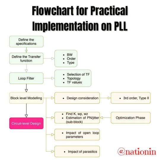
Dear IC designers, Flowchart of how a beginner should proceed with Phase locked Loop (PLL) design. It will help in practical implementation. ---------------------------------------------------------------------------------- Like👍 ll comments📝 II Share📢 ➡️Keep Supporting🙏 ---------------------------------------------------------------------------------- . . ---------------------------------------------------------------------------------- Follow (@nationin) for more stuff. ---------------------------------------------------------------------------------- . . _____________________________________________________ . #Intel #intelchips #neuromorphic #neuromorphichardware #diyprojects #electronicsprojects #electronics #xilinx #vivado #programming #verilog #vhdl #hdllanguauge #fpga #instagram #technology #vlsi #industry #tools #vivado #projects #start #intel #intelprocessors #gamingprocessors #gamingprocessors #nvidia #nvidiagaming #fpga #pll https://www.instagram.com/p/B_Q_gZYDuy-/?igshid=13pd726e0hi2r
#intel#intelchips#neuromorphic#neuromorphichardware#diyprojects#electronicsprojects#electronics#xilinx#vivado#programming#verilog#vhdl#hdllanguauge#fpga#instagram#technology#vlsi#industry#tools#projects#start#intelprocessors#gamingprocessors#nvidia#nvidiagaming#pll
0 notes
Link
Per voi che pensate in modo binario: no, non vi siete persi le parti da 1 al 4. Questa è una breve introduzione al dispositivo elettronico che preferisco: un array di porte programmabili sul campo (FPGA). Quando parlo degli FPGA, molti mi dicono: "Non so come funzionano", "Sono troppo complicati" o "Non posso programmarli in C". Poiché non mi piace vedere questi dispositivi così sorprendenti essere scherniti, cercherò di affrontare alcuni di questi problemi comuni di seguito e dissipare ogni dubbio.
Che cos'è un array di porte programmabili sul campo?
La risposta lunga: dal nome, si potrebbe dedurre che si tratta di una struttura programmabile di porte logiche. Più o meno, ma non del tutto, perché la matrice logica interna non è effettivamente implementata mediante porte. Definiamo invece i blocchi della matrice "elementi logici". Questi normalmente consistono di una tabella di ricerca (LUT) che implementa una funzione logica arbitraria e alcuni circuiti di supporto come multiplexer, sommatori e flip-flop. Spesso si parla di questa serie di elementi logici con il termine "il tessuto FPGA".
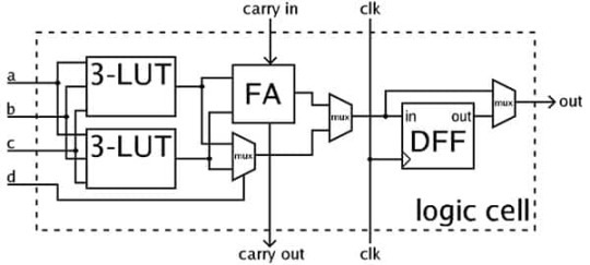
Figura 1: Esempio di un elemento logico FPGA. (Immagine per gentile concessione di Wikimedia Commons)
Per semplificare, mi piace pensare un FPGA come una scatola di elementi costitutivi colorati senza marchio per la creazione di circuiti digitali. Posso collegare i blocchi tra loro come mi pare per adattarli alla mia applicazione. Se sapete descrivere come si comporta un circuito digitale, potete crearlo all'interno di un FPGA con un numero di elementi logici sufficiente. Servono 25 uscite PWM? Nessun problema. Serve un protocollo di comunicazione speciale? Programma il codice hardware per gestirlo.
Perché dovrei avere bisogno di un FPGA?
Un FPGA viene utilizzato per implementare un sistema digitale, ma anche un semplice microcontroller può spesso date lo stesso risultato. I microcontroller sono economici e facili da inserire su una PCB. Gli FPGA sono strumenti potenti, ma potrebbero non essere adatti a tutti i casi. Hanno più requisiti di potenza, layout e di circuiti esterni e per questo possono essere proibitivi. L'uso di un FPGA sensibilmente più costoso e con molti requisiti speciali potrebbe sembrare ridicolo.
Ma potreste aver già indovinato il primo motivo per cui un FPGA è molto utile: la sua flessibilità. Avere blocchi logici configurabili significa non aver le mani legate in fatto di hardware. Non si esauriscono mai i timer o gli UART fintantoché vi sono elementi logici disponibili per crearne altri. Essere in grado di riconfigurare il progetto più avanti può anche estendere il ciclo di vita di un prodotto man mano la tecnologia e i requisiti che cambiano.
Il secondo motivo è la velocità. Un microcontroller esegue le istruzioni una alla volta, in modo sequenziale. Una struttura FPGA è intrinsecamente parallela a causa della sua natura hardware. Ciò consente che si verifichino varie cose simultaneamente, il che è utile per operazioni come FFT o l'elaborazione grafica che può essere costosa su un processore sequenziale. Gli FPGA hanno anche più opzioni I/O ad alta velocità rispetto a un tipico microcontroller come LVDS e transceiver con capacità di oltre 10 Gbps per protocolli come HDMI.
Come si programma un FPGA?
Gli FPGA usano un tipo speciale di linguaggio chiamato HDL o Hardware Description Language. È disponibile principalmente in due versioni: Verilog e VHDL. Quasi tutte le suite di sviluppo come Quartus o Vivado supporteranno entrambe per lasciarvi scegliere quella che preferite. Questi linguaggi sono quindi "sintetizzati", una procedura analoga alla compilazione per i microcontroller. Lo strumento di sintesi istruisce l'FPGA su come collegare i suoi elementi logici per creare l'effetto descritto dal codice programmato. Ricordare che il codice viene tradotto nell'hardware e non le istruzioni della CPU è molto importante all'inizio del lavoro.
Per semplificare lo sviluppo, i fornitori di FPGA offrono un catalogo di blocchi di codice di uso comune che possono essere facilmente inseriti in un progetto. Questi includono moltiplicatori, RAM, blocchi di comunicazione e molto altro che possono essere configurati e aggiunti a un progetto senza dover mai guardare il codice HDL in questione, accelerando i tempi di sviluppo.
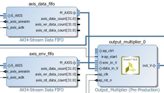
Figura 2: Diagramma a blocchi parziale che mostra i blocchi IP dal catalogo Xilinx e HLS. (Immagine per gentile concessione di eewiki.net)
Alcuni produttori offrono anche di strumenti di High Level Synthesis (HLS) in grado di tradurre una funzione scritta in C o C++ in un blocco di codice HDL. L'utilizzo di questi strumenti riduce notevolmente la barriera all'ingresso per gli sviluppatori con competenze software, poiché isolano da alcuni dettagli di basso livello.
Non siete ancora convinti? Una delle caratteristiche che preferisco di un FPGA è la possibilità di utilizzare un processore soft. Questo è un processore completo costruito con elementi logici dell'FPGA. Con questo, è possibile creare hardware di supporto personalizzato per il processore e scrivere la propria applicazione in C. Un semplice sistema con processore soft può essere impostato e programmato in pochi minuti. Se comunque serve un processore tradizionale, date un'occhiata ai SoC che integrano un processore FPGA e un processore ARM hard in un unico pacchetto.
Riassumendo, gli FPGA sono più costosi e più difficili da gestire rispetto a un tipico microcontroller, ma possono offrire molta più potenza e flessibilità nel caso serva. Man mano che la tecnologia migliora e gli FPGA diventano meno costosi con livelli di integrazione più elevati, potrebbero addirittura sostituire i microcontroller tradizionali. Quindi, se quanto ho detto vi alletta, iniziate a usare gli FPGA oggi stesso, per essere sempre al passo con i tempi. Se cercate una scheda di sviluppo a basso costo per iniziare, provate queste di vari nostri fornitori di FPGA: DE10-Lite di Terasic, Arty di Digilent, Mobile Dev Board di Lattice o Maker Kit di Microsemi.
1 note
·
View note
Text
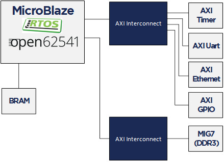
OPC UA server on a FPGA using open62541
Overview
Open Platform Communications Unified Architecture (OPC-UA - IEC62541) is a standardized platform-independent architecture which provides a service-based data exchange. In combination with TSN it allows new possibilities when it comes to high interoperability and deterministic communication.
Based on the open62541 implementation the following steps show how everything has to be setup to get it up and running on a FPGA (Artix7 with MicroBlaze). In combination with NetTimeLogic’s complete FPGA based TSN solution you get the full solution for industrial communication 4.0.
The example FPGA project and the application are available here:
https://github.com/NetTimeLogic/opcua
The open62541 implementation is available here:
https://github.com/open62541/open62541
Introduction
It is not straight forward to get the open62541 OPC UA stack up and running on an embedded system even if FreeRTOS and lwip is supported. The following implementation description is based on the open62541 documentation which describes how to build the library and how to implement a basic OPC UA server. The application creates an OPC UA server thread which is running under FreeRTOS with lwip.
The FPGA use a MicroBlaze softcore with DDR3, Axi Ethernet Lite, Axi Uart Lite AXI GPIO and AXI Timer. As hardware an Arty A7-100T development board from DIGILENT is used.
Required tools
To build the full project, the following tools are required:
Xilinx Vivado 2019.1
Xilinx SDK 2019.1
CMAKE (Python 2.7.x or 3.x)
UA Expert
BSP adjustments for LWIP
Open62541 supports “freertosLWIP” as an architecture. In that case it uses the libraries of the target device which are the ones of the BSP in Xilinx SDK.
To be able to compile the open62541 library some adjustments for the lwipopts.h file are needed:
Line 10-19 https://github.com/open62541/open62541/blob/master/arch/common/ua_lwip.h
Since this file is managed by the BSP in Xilinx SDK, manual modifications are overwritten when the BSP is generated. With the following workaround, it is possible to add the additional defines over the BSP setting GUI.
1. Go to: C:\Xilinx\SDK\2019.1\data\embeddedsw\ThirdParty\sw_services\lwip211_v1_0\data
2. Open the lwip211.tcl
3. Search the proc generate_lwip_opts {libhandle} and go to the end of this procedure
4. Add before the line puts $lwipopts_fd "\#endif" the following code:
#OPEN62541 implementation
set open62541_impl [expr [common::get_property CONFIG.open62541_impl $libhandle] == true]
if {$open62541_impl} {
puts $lwipopts_fd "\#define LWIP_COMPAT_SOCKETS 0"
puts $lwipopts_fd "\#define LWIP_SOCKET 1"
puts $lwipopts_fd "\#define LWIP_DNS 1"
puts $lwipopts_fd "\#define SO_REUSE 1"
puts $lwipopts_fd "\#define LWIP_TIMEVAL_PRIVATE 0"
puts $lwipopts_fd ""
}
5. Save the file
6. Open the file lwip211.mld
7.Add the new Parameter e.g. at line 47:
PARAM name = open62541_impl, desc = "Used as an open62541 implementation?", type = bool, default = false;}
8.Save the file
9. Restart Xilinx SDK
After this change and a restart of Xilinx SDK the new option will be visible in the BSP settings GUI of the lwip.
Design preparation
Before everything is ready to build the open62541 library, the implemented FPGA design from Xilinx Vivado and a software application project in Xilinx SDK is needed. In this example project a MicroBlaze design with DDR3 is used (unfortunately the application does not fit into the available block RAM).
Vivado
The Vivado project can be created with the available tcl script. By running the implementation of the Vivado project the bitstream can be created. With File->Export->Export Hardware the hardware definition can be created.
File->Launch SDK starts the SDK.
Xilin SDK
In Xilinx SDK a new empty Application Project with the OS Platform “freertos10_xilinx” can be created.
File->New->Application Project.
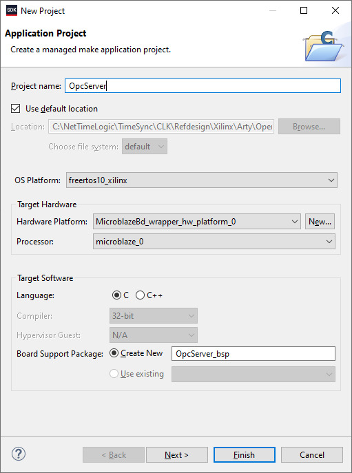
After the project is created some adjustments in the OpcServer_bsp are needed
Select lwip211 as supported libraries
Go to the lwip211 and adjust following parameter:
api_mode = socket_API
open62541_impl = true
Go to the freertos20_xilinx and adjust the following parameters:
Check_for_stack_overflow = 1
total_heap_size = 2097152
Re-generate BSP sources
The environment is now ready to start with CMake.
CMake
The easiest way is to work with the CMake GUI. Later it can be used in Xilinx SDK.
CMake for open62541 is used with following adjustment:
UA_ENABLE_AMALGAMATION = ON
UA_ENABLE_HARDENING = OFF
UA_ARCH_EXTRA_INCLUDES = <path to microblaze/include>
UA_ARCH_REMOVE_FLAGS = -Wpedantic -Wno-static-in-inline -Wredundant-decls
CMAKE_C_FLAGS = -Wno-error=format= -mlittle-endian -DconfigUSE_PORT_OPTIMISED_TASK_SELECTION=0 -DconfigAPPLICATION_ALLOCATED_HEAP=3 -DUA_ARCHITECTURE_FREERTOSLWIP
UA_LOGLEVEL = 100 (optional for debugging)
1. Start the CMake GUI
2. Select the correct source code path where the open62541 GIT repository is located and define the path where you want to build the binaries:

3. Click Configure:
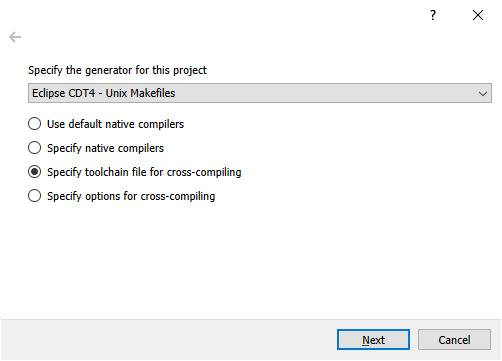
4. Select the CMake file which defines the compilation toolchain and other settings:

5. Click again on Configure and after that on Generate
6. The Unix Makefiles are now ready and can be added Xilinx SDK workspace:
File->Open Projects from File system
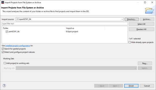
7. Now it should be possible to generate the open62541.c/h file in Xilinx SDK.
Make Target->all
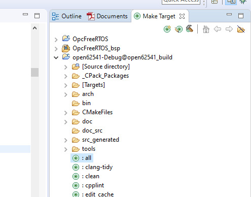
8. The workspace should have now following structure:

Creating the OPC UA server application
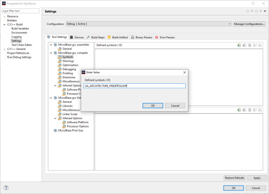
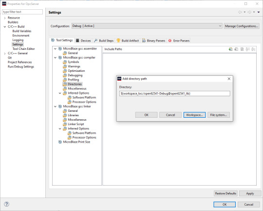
C/C++ Build settings
For a compilation without errors some adjustments in the application project Build settings are required.
1. Add the symbol for UA_ARCHITECTURE_FREERTOSLWIP
2. Add the open62541 build directory as include path
3. Add the open62541 build directory as library search path
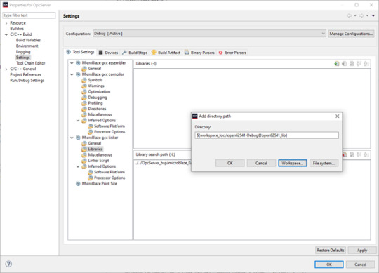
4. Link the folder to the source location of open62541.c/h

5. Add an exclusion pattern that only the open62541.c/h are used:

Linker script
The linker script for our OPC UA server application needs some small adjustments.
With Xilinx->Generate linker script a new lscript.ld with following settings can be created:
Heap Size: (min) 1MB
Stack Size: (min) 1MB

Now the application project should be ready for a successful compilation.
OPC UA Server app
The complate Workspace is here available:
https://github.com/NetTimeLogic/opcua/tree/master/Src/Sdk_workspace
In Xilinx SDK the source file OpcServer.c can be imported to the OpcServer application project.
The thread stack size is defined with 4096 it might be possible that the application is not running properly with other values. However, the hook functions for MallocFailed or StackOverflow might be helpful.
In a first step the network initialization is done. This includes auto negotiation, ip configuration, interface binding and starting the lwip receive thread. After that the opcua thread gets started.
Important for a working server is the configuration and especially the buffer size of the network layer. With the following settings, the server was running without any problems:
config->networkLayers->localConnectionConfig.recvBufferSize = 32768; config->networkLayers->localConnectionConfig.sendBufferSize = 32768; config->networkLayers->localConnectionConfig.maxMessageSize = 32768;
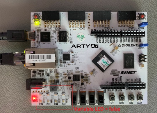
Before the server is started an object and a variable are added to the server. Additionally, a callback for the variable is configured, which allows to control the LEDs on the ArtyA7 board by an OPC client. After that the server gets started and runs until the running variable is set to false (never in this case).
Connecting to the OPC UA Server
After a successful implementation of the MicroBlaze FPGA design, building the open62541 library and compiling the OPC UA server application everything is ready.
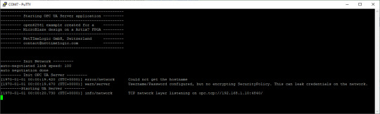
The Arty A7 board should be connected to the PC over USB and the RJ45 is connected to a network interface adapter.
1. Open a serial terminal for the debug print out (baud rate: 115200)
2. Loading the bitstream (from Vivado or SDK)
3. Run the Application (from SDK)
4. If the application has successfully started, in the serial terminal following text is printed out:
5. Start UaExpert
6. Add the server via “Custom Discovery” with the configured open62541 hostname
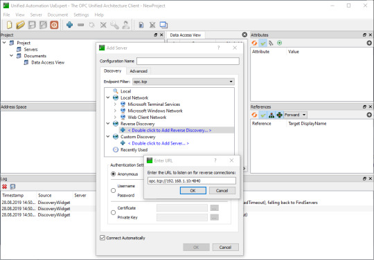
7. Expand the added server to add the connection. In the serial terminal you get already some information that a new connection over TCP was detected
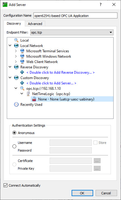
8. After a successful connection in UaExpert the defined object a variable are visible.
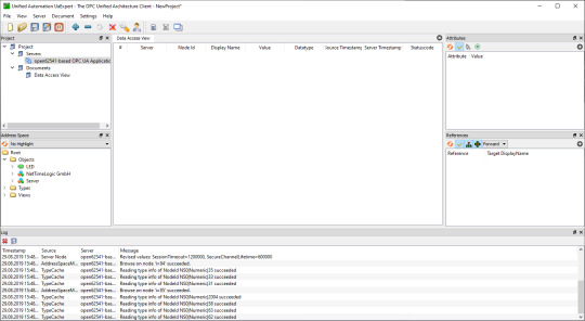
9. The variable LED can now be added to the Data Access View via drag & drop
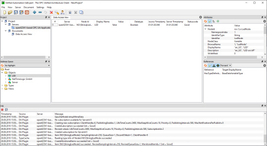
10. By changing the boolean value of the variable, the LEDs on the ArtyA7 can be switched on /off.

Summary
To get an open62541 server running on a MicroBlaze softcore following adjustments are needed:
Add the defines in the lwip BSP for lwipopts.h:
#define LWIP_COMPAT_SOCKETS 0
#define LWIP_SOCKET 1
#define LWIP_DNS 1
#define SO_REUSE 1
#define LWIP_TIMEVAL_PRIVATE 0
Adjust the BSP settings for lwip:
api_mode = socket_API
open62541_impl = true
Adjust the BSP settings for FreeRTOS:
Check_for_stack_overflow = 1
total_heap_size = 2097152
Adjust CMake options for open62541:
UA_ENABLE_AMALGAMATION = ON
UA_ENABLE_HARDENING = OFF
UA_ARCH_EXTRA_INCLUDES = <path to microblaze/include>
UA_ARCH_REMOVE_FLAGS = -Wpedantic -Wno-static-in-inline
-Wredundant-decls
CMAKE_C_FLAGS = -Wno-error=format= -mlittle-endian
-DconfigUSE_PORT_OPTIMISED_TASK_SELECTION=0
-DconfigAPPLICATION_ALLOCATED_HEAP=3
-DUA_ARCHITECTURE_FREERTOSLWIP
UA_LOGLEVEL = 100 (optional for debugging)
Generate a linker script with at least: 1MB heap and 1MB stack
Adjust the C/C++ build settings / include sources/libraries
Define the thread stack size to 4096
Adjust the buffer size of the server config:
config->networkLayers->localConnectionConfig.recvBufferSize = 32768;
config->networkLayers->localConnectionConfig.sendBufferSize = 32768;
config->networkLayers->localConnectionConfig.maxMessageSize = 32768;
1 note
·
View note
Text
Lab 1: Introduction to ModelSim and Vivado with the Design of Barrel Shifter Solution
Lab 1: Introduction to ModelSim and Vivado with the Design of Barrel Shifter Solution
Introduction
SHIFT
X0
X1
X2
X3
COUNT
SHIFT 3
Y3
D
SHIFT 2
Y2
E
C
O
SHIFT 1
Y1
D
E
SHIFT 0
R
Y0
Figure 1 Schematic of a 4-bit crossbar barrel shifter.
(Source: https://en.wikipedia.org/wiki/File:Crossbar_barrel_shifter.svg)
The purpose of this lab is to get acquainted with the Mentor Graphics ModeSim and Xilinx
Vivado toolchain through a Simple Design. A barrel shifter is a…

View On WordPress
0 notes
Text
ECE Lab 1: Introduction to ModelSim and Vivado with the Design of Barrel Shifter Solution
ECE Lab 1: Introduction to ModelSim and Vivado with the Design of Barrel Shifter Solution
Introduction
SHIFT
X0
X1
X2
X3
COUNT
SHIFT 3
Y3
D
SHIFT 2
Y2
E
C
O
SHIFT 1
Y1
D
E
SHIFT 0
R
Y0
Figure 1 Schematic of a 4-bit crossbar barrel shifter.
(Source: https://en.wikipedia.org/wiki/File:Crossbar_barrel_shifter.svg)
The purpose of this lab is to get acquainted with the Mentor Graphics ModeSim and Xilinx
Vivado toolchain through a Simple Design. A barrel shifter is a…

View On WordPress
0 notes
Text
MIPS Single-Cycle Datapath and Controller & Experiments on SystemVerilog Solution
MIPS Single-Cycle Datapath and Controller & Experiments on SystemVerilog Solution
Purpose: Understanding the design of the Single-Cycle MIPS Processor: What are the roles of each module in the datapath and the control units, how do control signals dictate the behavior of the processor.
Summary
Part 1 (50 points): Understanding modules in the single-cycle processor architecture, preparation for the Xilinx Vivado simulations of the single-cycle MIPS processor.
Part 2 (50…

View On WordPress
0 notes
Last Seen Blogs

ratpyramid
I became the ants and all I got was this t-shirt

erencan16c
Eren Can
erencan16c
Eren Can
erencan16c
Eren Can

potterwholock
I will make you into shoes. Or maybe a purse.