#VHDL Architecture
Text
youtube
VHDL Tutorial : Your First VHDL Design: VHDL Entity & Architecture - A Beginner's Guide
Welcome to the ultimate beginner's guide for Your First VHDL Design! In this video, we will dive into the fundamentals of VHDL Entity and Architecture and provide you with a comprehensive understanding of the topic. Whether you are new to VHDL or looking to refresh your knowledge, this guide is designed to help you get started and pave your way to becoming an expert VHDL designer. In this tutorial, we will cover the basics of VHDL, starting with the VHDL Entity and its crucial role in the design process. You will learn how to define and describe the inputs and outputs of your VHDL design using the Entity section, providing the necessary specifications for your project. Moving on, we will explore the VHDL Architecture, which defines the actual implementation of your design. Through a step-by-step walkthrough, you will discover how to construct the architecture block by block, ensuring a well-structured and functional VHDL design. To make the learning experience more practical, we will dive into real-world examples and demonstrate each concept using a popular VHDL software tool. You'll witness the transition from theory to practice, gaining hands-on experience in VHDL design. With this beginner's guide, you'll not only grasp the essentials of VHDL Entity and Architecture but also acquire the ability to kickstart your own VHDL designs, opening up a wide range of possibilities in digital circuit design. Subscribe to our channel for more exciting VHDL tutorials and stay tuned for upcoming videos in this series where we will explore advanced VHDL concepts and applications.
Subscribe to "Learn And Grow Community"
YouTube : https://www.youtube.com/@LearnAndGrowCommunity
LinkedIn Group : https://www.linkedin.com/groups/7478922/
Blog : https://LearnAndGrowCommunity.blogspot.com/
Facebook : https://www.facebook.com/JoinLearnAndGrowCommunity/
Twitter Handle : https://twitter.com/LNG_Community
DailyMotion : https://www.dailymotion.com/LearnAndGrowCommunity
Instagram Handle : https://www.instagram.com/LearnAndGrowCommunity/
Follow #LearnAndGrowCommunity
#VHDL#VHDL Entity#VHDL Architecture#VHDL Design#Beginner's Guide#Digital Circuit Design#VHDL Tutorial#VHDL Basics#VHDL Examples#VHDL Software#Learn VHDL#VHDL Learning#VHDL Step-by-step#VHDL Introduction#VHDL Fundamentals#VHDL Engineering#Hardware Design#Circuit Design#Xilinx ISE#Xilinx Vivado#Digital#ASIC#Engineering#Students#Training#Tutorial#Altera#Hardware description language#modeling style#data flow
1 note
·
View note
Text
High Performance FPGA Solutions

In today's rapidly evolving technological landscape, the demand for high-performance solutions is ever-increasing. Field-Programmable Gate Arrays (FPGAs) have emerged as versatile tools offering customizable hardware acceleration for a wide range of applications. Let's delve into the world of high performance FPGA solutions, exploring their key features, applications, challenges, recent advances, case studies, and future trends.
Introduction to High Performance FPGA Solutions
Definition of FPGA
Field-Programmable Gate Arrays (FPGAs) are semiconductor devices that contain an array of programmable logic blocks and configurable interconnects. Unlike Application-Specific Integrated Circuits (ASICs), FPGAs can be programmed and reprogrammed after manufacturing, allowing for flexibility and customization.
Importance of High Performance in FPGA Solutions
High performance is crucial in FPGA solutions to meet the demanding requirements of modern applications such as real-time data processing, artificial intelligence, and high-frequency trading. Achieving optimal speed, throughput, and efficiency is paramount for maximizing the effectiveness of FPGA-based systems.
Key Features of High Performance FPGA Solutions
Speed and Throughput
High performance FPGA solutions are capable of executing complex algorithms and processing vast amounts of data with exceptional speed and efficiency. This enables real-time decision-making and rapid response to dynamic inputs.
Low Latency
Reducing latency is essential in applications where response time is critical, such as financial trading or telecommunications. High performance FPGAs minimize latency by optimizing data paths and processing pipelines.
Power Efficiency
Despite their high performance capabilities, FPGA solutions are designed to operate within strict power constraints. Advanced power management techniques ensure optimal performance while minimizing energy consumption, making FPGAs suitable for battery-powered or energy-efficient devices.
Flexibility and Reconfigurability
One of the key advantages of FPGAs is their inherent flexibility and reconfigurability. High performance FPGA solutions can adapt to changing requirements by reprogramming the hardware on-the-fly, eliminating the need for costly hardware upgrades or redesigns.
Applications of High Performance FPGA Solutions
Data Processing and Analytics
FPGAs excel in parallel processing tasks, making them ideal for accelerating data-intensive applications such as big data analytics, database management, and signal processing.
Artificial Intelligence and Machine Learning
The parallel processing architecture of FPGAs is well-suited for accelerating AI and ML workloads, including model training, inference, and optimization. FPGAs offer high throughput and low latency, enabling real-time AI applications in edge devices and data centers.
High-Frequency Trading
In the fast-paced world of financial markets, microseconds can make the difference between profit and loss. High performance FPGA solutions are used to execute complex trading algorithms with minimal latency, providing traders with a competitive edge.
Network Acceleration
FPGAs are deployed in network infrastructure to accelerate packet processing, routing, and security tasks. By offloading these functions to FPGA-based accelerators, network performance and scalability can be significantly improved.
Challenges in Designing High Performance FPGA Solutions
Complexity of Design
Designing high performance FPGA solutions requires expertise in hardware architecture, digital signal processing, and programming languages such as Verilog or VHDL. Optimizing performance while meeting timing and resource constraints can be challenging and time-consuming.
Optimization for Specific Tasks
FPGAs offer a high degree of customization, but optimizing performance for specific tasks requires in-depth knowledge of the application domain and hardware architecture. Balancing trade-offs between speed, resource utilization, and power consumption is essential for achieving optimal results.
Integration with Existing Systems
Integrating FPGA-based accelerators into existing hardware and software ecosystems can pose compatibility and interoperability challenges. Seamless integration requires robust communication protocols, drivers, and software interfaces.
Recent Advances in High Performance FPGA Solutions
Improved Architectures
Advancements in FPGA architecture, such as larger logic capacity, faster interconnects, and specialized processing units, have led to significant improvements in performance and efficiency.
Enhanced Programming Tools
New development tools and methodologies simplify the design process and improve productivity for FPGA developers. High-level synthesis (HLS) tools enable software engineers to leverage FPGA acceleration without requiring expertise in hardware design.
Integration with Other Technologies
FPGAs are increasingly being integrated with other technologies such as CPUs, GPUs, and ASICs to create heterogeneous computing platforms. This allows for efficient partitioning of tasks and optimization of performance across different hardware components.
Case Studies of Successful Implementation
Aerospace and Defense
High performance FPGA solutions are widely used in aerospace and defense applications for tasks such as radar signal processing, image recognition, and autonomous navigation. Their reliability, flexibility, and performance make them ideal for mission-critical systems.
Telecommunications
Telecommunications companies leverage high performance FPGA solutions to accelerate packet processing, network optimization, and protocol implementation. FPGAs enable faster data transfer rates, improved quality of service, and enhanced security in telecommunication networks.
Financial Services
In the highly competitive world of financial services, microseconds can translate into significant profits or losses. High performance FPGA solutions are deployed in algorithmic trading, risk management, and low-latency trading systems to gain a competitive edge in the market.
Future Trends in High Performance FPGA Solutions
Increased Integration with AI and ML
FPGAs will play a vital role in accelerating AI and ML workloads in the future, especially in edge computing environments where low latency and real-time processing are critical.
Expansion into Edge Computing
As the Internet of Things (IoT) continues to grow, there will be increasing demand for high performance computing at the edge of the network. FPGAs offer a compelling solution for edge computing applications due to their flexibility, efficiency, and low power consumption.
Growth in IoT Applications
FPGAs will find widespread adoption in IoT applications such as smart sensors, industrial automation, and autonomous vehicles. Their ability to handle diverse workloads, adapt to changing requirements, and integrate with sensor networks makes them an ideal choice for IoT deployments.
Conclusion
In conclusion, high performance FPGA solutions play a crucial role in driving innovation and accelerating the development of advanced technologies. With their unparalleled speed, flexibility, and efficiency, FPGAs enable a wide range of applications across industries such as aerospace, telecommunications, finance, and IoT. As technology continues to evolve, the demand for high performance FPGA solutions will only continue to grow, shaping the future of computing.
0 notes
Text
Intel FPGAs speed up databases with oneAPI and SIMD orders
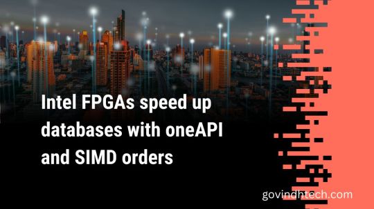
A cutting-edge strategy for improving single-threaded CPU speed is Single Instruction Multiple Data (SIMD).
FPGAs are known for high-performance computing via customizing circuits for algorithms. Their tailored and optimized hardware accelerates difficult computations.
SIMD and FPGAs seem unrelated, yet this blog article will demonstrate their compatibility. By enabling data parallel processing, FPGAs can boost processing performance with SIMD. For many computationally intensive activities, FPGA adaptability and SIMD efficiency are appealing.
High-performance SIMDified programming
SIMD parallel processing applies a single instruction to numerous data objects. Special hardware extensions can execute the same instruction on several data objects simultaneously.
SIMDified processing uses data independence to boost software application performance by rewriting application code to use SIMD instructions extensively.
Key advantages of SIMDified processing include:
Increased performance: SIMDified processing boosts computationally intensive software applications.
Integrability: Intrinsics and dedicated data types make SIMDified processing desirable.
SIMDified processing is available on many current processors, giving it a viable option for computational speed improvement.
Despite its benefits, SIMDified processing is not ideal for many applications. Applications with minimal data parallelism will not benefit from SIMDified processing. It is a convincing method for improving data-intensive software applications.
SIMD Portability Supports Heterogeneity
SIMD registers and instructions make up SIMD instruction sets. SIMD intrinsics in C/C++ are the best low-level programming method for performance.
Low-level programming in heterogeneous settings with different hardware platforms, operating systems, architectures, and technologies is difficult due to hardware capabilities, data parallelism, and naming standards.
Specialized implementations limit portability between platforms, hence SIMD abstraction libraries provide a common SIMD interface and abstract SIMD functions. These libraries use C++ template metaprogramming and function template specializations to translate to SIMD intrinsics and potential compensations for missing functions, which must be implemented.
C/C++ libraries let developers construct SIMD-hardware-oblivious application code and SIMD extension code with minimum overhead. Separating SIMD-hardware-oblivious code with a SIMD abstraction library simplifies both sides.
This method has promoted many SIMD libraries and abstraction layers to solve problems:
Examples of SIMD libraries
Google Highway (open-source)
Xsimd (C++ wrapper for SIMD instances)
Such libraries allow SIMDified code to be designed once and specialized for the target SIMD platform by the SIMD abstraction library. Libraries and varied design environments suit SIMD instructions and abstraction.
Accelerating with FPGAs
FPGAs speed software at low cost and power. Traditional FPGAs required a strong understanding of digital design concepts and specific languages like VHDL or Verilog. FPGA-based solutions are harder to access and more specialized than CPU or GPU-based computing platforms due to programming complexity and code portability. Intel oneAPI changes this.
Intel oneAPI is a software development kit that unifies CPU, GPU, and FPGA programming. It supports C++, Fortran, Python, and Data Parallel C++ (DPC++) for heterogeneous computing to improve performance, productivity, and development time.
Since Intel oneAPI can target FPGAs from SYCL/C++, software developers are increasingly interested in using them for data processing. FPGAs can be used with SIMDified applications by adding them as a backend to the SIMD abstraction library. This allows SIMD applications with FPGAs.
SIMD and FPGAs go together
Annotations let the Intel DPC++ compiler synthesis C++ code into circuits and auto-vectorize data-parallel processing. Annotating and implementing code arrays as registers on an FPGA removes data access constraints and allows parallel processing from sink to source. This enables SIMD performance acceleration using FPGAs straightforward and configurable.
SIMD abstraction libraries are a logical choice for FPGA SIMD processing. As noted, the libraries support Intel and ARM SIMD instruction set extensions. TSL abstraction library simplifies FPGA SIMD instruction implementation in the following example. The scalar code specifies loading registers, and the pragma unroll attribute tells the DPC++ Compiler to implement all pathways in parallel in the generic element-wise addition example below.
This simple element-wise example has no dependencies, and comparable implementations will work for SIMD instructions like scatter, gather, and store. Optimization can also accelerate complex instructions.
A horizontal reduction requires a compile-time adder tree of depth ld(N), where N is the number of entries. Unroll pragmas with compile-time constants can implement adder trees in a scalable manner, as shown in the following code example.
Software that calls a library of comparable SIMD components can expedite SIMD instructions on Intel FPGAs by adding the examples above.
Intel FPGA Board Support Package adds system benefits. Intel FPGAs use a BSP to describe hardware interfaces and offer a kernel shell.
The BSP enables SYCL Universal Shared Memory (USM), which frees the CPU from data transfer management by exchanging data directly with the accelerator. FPGAs can be coprocessors.
The pre-compiled BSP generates only kernel logic live, reducing runtime.
Intel FPGAs are ideal for SIMD and streaming applications like current composable databases because to their C++/SYCL compatibility, CPU data transfer offloading, and pre-compiled BSPs.
SIMD/FPGA simplicity
At SiMoDSIGMOD 2023 in Seattle, USA, Dirk Habich, Alexander Krause, Johannes Pietrzyk, and Wolfgang Lehner of TU Dresden presented their paper “Simplicity done right for SIMDified query processing on CPU and FPGA” on using FPGAs to accelerate SIMD instructions. The work, supported by Intel’s Christian Färber, illustrates how practical and efficient developing a SIMDified kernel in an FPGA is while achieving top performance.
The paper evaluated FPGA acceleration of SIMD instructions using a dual-socket 3rd-generation Intel Xeon Scalable processor (code-named “Ice Lake”) with 36 cores and a base frequency of 2.2 GHz and a BitWare IA-840f acceleration card with an Intel Agilex 7 AGF027 FPGA and 4x 16 GB DDR4 memories.
First, they gradually increased the SIMD instance register width to see how it affected maximum acceleration bandwidth. The first instance, a simple aggregation, revealed that the FPGA accelerator’s bandwidth improves with data width doubling until the global bandwidth saturates an ideal acceleration case.
The second scenario, a filter-count kernel with a data dependency in the last stage of the adder tree, demonstrated similar behavior but saturates earlier at the PCIe link width. Both scenarios demonstrate the considerable speeding gains of natively parallel instructions on a highly parallel architecture and suggest that wide memory accesses could sustain the benefits.
Final performance comparisons compared the FPGA and CPU. CPU and FPGA received the same multi-threaded AVX512-based filter-count kernel. As expected, per-core CPU bandwidth decreased as thread count and CPU core count grew. FPGA performance was peak across all workloads.
Based on this work, the TU Dresden and Intel team researched how to use TSL to use an FPGA as a bespoke SIMD processor.
Read more on Govidhtech.com
0 notes
Text
Subjects/Courses in Degree Of Information technology (IT) - ACEIT
BTech IT syllabus is a mix of theory and practical knowledge. The BTech IT 1st year syllabus at best engineering colleges in Jaipur covers the primary science, math, and engineering subjects. In the 2nd year syllabus, the B. Tech IT programme touches upon the specialized and elective subjects. Important B. Tech IT subjects include digital electronics, programming language, electronic mathematics, etc. For B. Tech IT jobs, graduates become adept at the latest new technologies, arriving at the most optimal solutions (consuming less time and effort) for any technological problems that might occur, whether small or large.
This course is divided into 4 years, 8 semesters that are 2 semesters each year. The marks of the students are based on their performances, in theory, lab work, and research projects assigned to them.
Apart from the chief course, the students of top engineering colleges Jaipur have to study a parallel course which instills helps them in improving and sharpening their skills. The course may also comprise of lectures, tutorials, training, research projects, and workshops. This helps students to learn more. Moreover, it helps in getting hands-on subjects like Discrete Structures, Web Technologies, Android Applications Development, Artificial Intelligence, Design and Analysis of Algorithm, and many other subjects.
Semester-Wise Syllabus For B.Tech IT
B. Tech IT course syllabus is made up of 8 semesters in 4 years. Students study core subjects in the first year and then move to elective subjects according to their interest in the second year. The course also focuses on practical learning through projects and internships. Semester wise subjects are as follows:
1. First Year Syllabus
a. Semester Ⅰ – It includes subjects like Applied Mathematics, Environment Studies, Engineering Mathematics, Electrical Science, Applied Physics Lab, Programming in C Lab, Engineering Graphics Lab, Engineering Mechanics Lab, English.
b. Semester Ⅱ – It includes subjects like Applied Mathematics, Applied Physics - II (Modern Physics), Data Structures using C, Applied Chemistry, Elements of Mechanical Engineering, Data Structures Using C Lab, English, Engineering Mechanics, Engineering Graphics.
2. Second Year Syllabus
a. Semester Ⅲ – It includes subjects like Analog Electronics, Database Management Systems, Operating Systems, Object-Oriented Programming using C++, Applied Mathematics – III, Analog Electronics Lab, UNIX Programming Lab – I.
b. Semester Ⅳ – It include subjects like Discrete Mathematics, Communication Systems, Computer Graphics, Management Information System, Digital Electronics, Digital Electronics Lab, Communication Systems Lab.
3. Third Year Syllabus
a. Semester Ⅴ – It include subjects like Software Engineering, VHDL Programming, Computer Architecture, Data Communication & Computer Networks, Java Programming, VHDL Programming Lab, Software Engineering Lab.
b. Semester Ⅵ – It include subjects like Microprocessor, System Programming, E-Commerce and ERP, Advanced Networking, Advanced Java programming, System Programming Lab, Microprocessor Lab.
4. Fourth Year Syllabus
a. Semester Ⅶ – It include subjects like Artificial Intelligence, Programming with ASP.Net, Software Project Management, Advance DBMS, Operational Research Lab, Mobile Computing, Information Security, Grid Computing.
b. Semester Ⅷ – It include subjects like Digital Image Processing, Information Storage & Management, Project Submission, Comprehension Viva-voce, Network Operating System, Linux Administration, Software Testing & Quality Assurance, Real-time systems.
Types Of Subjects In B. Tech IT
B. Tech IT at best BTech colleges Jaipur includes two kinds of subjects like core and the elective subjects. Along with this, internship and project submissions are included. In this course, students learn through group discussions and presentations prepared by themselves.
a. Core subjects - Some core subjects involve Engineering Mathematics, Basics of Electronics, Computer Languages, Introduction to Web Technology, Operating Systems, Concepts of Database, Software Project Management, Introduction to Microprocessor, Computer Graphics and Simulation, Data Mining and Data Warehousing.
b. Lab Subjects – Some lab subjects like VHDL Programming Lab, Programming with ASP.Net, Software Engineering Lab, System Programming Lab, Microprocessor Lab.
c. Elective Subjects – Some elective subjects include Introduction to Linux, Penetration Testing, Information Assurance and Security Management for IT, Network Programming, Network Security and Firewalls, Data and Information Security, Human Security, Malware Analysis, Mobile and Wireless Security.
Course Structure For B. Tech IT
B. Tech IT syllabus at engineering colleges Jaipur focuses on building holistic learning of information technology. In the first year, subjects are similar to aspirant studies in class 12. From the second year, core and elective subjects form the main course of the curriculum. In this way, students can choose the topics which are of interest to them. The course structure is a mix of theoretical knowledge and practical use of this knowledge through projects, research papers, group discussions, and internships. The course structure includes Ⅳ Semesters, Core and Elective Subjects, Research Papers, Surveys, Practical, Thesis Writing, Seminars, Projects, etc.
Teaching Methodology And Techniques
Teaching methodology for the students of BTech IT college Jaipur has a mixture of both theoretical as well as practical knowledge. This teaching methodology helps in building a comprehensive understanding of information technology. Through this methodology, students can understand the world of coding, networking, app development, cybersecurity, etc. Some methodology techniques used by colleges are Discussions, Problem-based Projects, E-learning, Co-curricular Activities, Field Trips, Practical Learnings.
Important Facts For Information Technology
This four-year course at private engineering colleges in Jaipur is divided into 8 semesters. The marks are rewarded according to the number of subjects in each semester.
Subjects related to Data Structures and Algorithms, Operating Systems, Parallel Computing, Artificial Intelligence, Computer Graphics, Soft Computing, Genetic Algorithms, Bioinformatics, Virtual Reality, Cloud Computing, Semantic Web Technologies, Software Architecture, Simulation and Modelling, Advances Database Structures, etc., are part of this course.
These subjects help the students gain an insight into various developments in technology and their applications in computer science engineering. A lot of innovation and self-equipped skills would be essential for the duration of this course. Much research and improvisation are required to keep up with the growing trend of producing unique technologies.
Every student of BTech college must score the minimum score to complete the respective course. Everyone should need to undertake a final year project as well. The type and the duration of the project, along with the respective credit score, are decided by the university/college.
Besides the respective core subjects, a student is free to take up elective courses as well. It is based on their interest and choices. A student can opt-in for such electives at the beginning of any semester at their own discretion. The choices of such electives may vary based on colleges or universities.
0 notes
Text
vhdl
this stands for vhsic hardware description language. (vhsic stands for very high speed integrated circuit.) it does not program a sequence of steps like a typical programming language, instead it describes a circuit.
The language is very simple, but it is not as human readable as language such as Java or Python.
When describing a circuit in vhdl, you always need 3 components. These are (1) the library statements, (2) the entity clause (3) the architecture.
The library statements import things you may need for circuit, such as standard digital logic components. The entity statement describes the circuit’s ports, and the architecture describes it behavior and its composition.
1 note
·
View note
Text
Houston Texas Appliance Parts: How Efinix is Conquering the Hurdle of Hardware Acceleration for Devices at the Edge
Houston Texas Appliance Parts
How Efinix is Conquering the Hurdle of Hardware Acceleration for Devices at the Edge
by Houston Texas Appliance Parts on Tuesday 07 March 2023 08:21 AM UTC-05
In previous articles, we established the many ways FPGAs surpass other AI chipsets for running machine learning algorithms at the edge in terms of reconfigurability, power consumption, size, speed, and cost. Moreover, how the microarchitecture-agnostic RISC-V instruction set architecture (ISA) marries up with the architectural flexibility of the FPGA seamlessly. However, the apparent lack of mid-range, cost-effective FPGAs and their less-than-straightforward design flow are a major bottleneck — the software skills required for the fully custom hardware description language (HDL) implementation are difficult to find and often come with a steep learning curve.
Efinix fills the gap with FPGAs built on the innovative quantum compute fabric made up of reconfigurable tiles known as exchangeable logic and routing (XLR) cells that function as either logic or routing, rethinking the traditional fixed ratio of logic elements (LEs) and routing resources. This allows for a high-density fabric in a small device package where no part of the FPGA is underutilized. The potential of this platform transcends the typical barriers facing edge-based devices today: power consumption, latency, cost, size, and ease of development.
Possibly the most striking feature of Efinix FPGAs is the ecosystem and state-of-the-art tool flow surrounding it that lowers development barriers, allowing designers to readily implement AI at the edge using the same silicon — from prototype to production. Efinix has embraced the RISC-V, thereby allowing users to create applications and algorithms in software — capitalizing on the ease of programmability of this ISA without being bound to proprietary IP cores such as ARM. Since this is all done with flexible FPGA fabric, users can massively accelerate in hardware. Efinix offers support for both low level and more complex custom instruction acceleration. Some of these techniques include the TinyML accelerator and predefined hardware accelerator sockets. With approaches such as these, the leaps in acceleration accomplished delivers hardware performance while retaining a software-defined model that can be iterated and refined without the need to learn VHDL. This results in blazing-fast speeds for edge devices, all while consuming low power and functioning within a small footprint. This article discusses precisely how the Efinix platform simplifies the entire design and development cycle, allowing users to take advantage of the flexible FPGA fabric for a scalable embedded processing solution.
Barriers at the edge — a dam-blocking progress
From massive wireless sensor networks to streaming a high-resolution 360o immersive AR or VR experience, most of the world's data lies at the edge. Disaggregating the compute burden from the cloud and bringing it closer to the devices opens doors for next-generation, bandwidth-hungry, ultra-low-latency applications in autonomous driving, immersive digital experiences, autonomous industrial facilities, telesurgery, and so on. The use cases are endless once the enormous roadblock of transmitting data to and from the cloud is sidestepped.
However, the very defining factors of low-latency, power-hungry compute at the edge are the very same factors that pose a significant design challenge for these small but prolific power-limited devices. How then is it possible to design a device capable of processing the power-hungry relevant ML algorithms without having to invest in elaborate technologies? The solution has been to implement any hardware deemed sufficient to run the suitable applications and algorithms (e.g., CPU, GPU, ASIC, FPGA, ASSP) while accelerating the more compute-intensive tasks to balance the compute time (latency) and resources used (power consumed).
As with any innovation, the landscape of deep learning is continually shifting with updating models and optimization techniques, necessitating the use of more agile hardware platforms that can change almost as rapidly as the programs running on them with little to no risk. The parallel processing and flexibility/reconfigurability of FPGAs seem to line up seamlessly with this need. However, making these devices available for mainstream, high-volume applications requires lowering the design barriers for configuring and accelerating the FPGA fabric — a time-consuming process that normally requires a high degree of expertise. Furthermore, traditional accelerators are typically not granular enough and incorporate large pieces of a model that typically do not scale well. They also generally consume far too much power and are, more often than not, proprietary — causing engineers to relearn how to use the vendor-specific platform.
The Sapphire RISC-V core
Creating an application on the RISC-V Core in C/C++
Efinix squarely addresses all of these potential obstacles by taking on the challenge of making FPGAs available to the AI/ML community in an intuitive way. The RISC-V Sapphire core is fully user configurable through the Efinity GUI; this way, users do not have to know all the VHDL behind implementing the RISC-V in the FPGA and can exploit the straightforward programmability of common software languages (e.g., C/C++). This allows teams to rapidly generate applications and algorithms in software at speed. All the required peripherals and buses can be specified, configured, and instantiated alongside the Sapphire core to deliver a fully configured SoC (Figure 1). This RISC-V capability includes multi-core (up to four cores) support and Linux capability, delivering a high-performance processor cluster to a designer's FPGA application as well as the ability to run applications directly on the Linux operating system. The next step — hardware acceleration — is greatly simplified with hardware-software partitioning; once a designer has perfected their algorithm in software, they can progressively start to accelerate this within the flexible Efinix FPGA fabric. However, before we move on to the next step of hardware acceleration, it would be important to understand the inherent benefits of the RISC-V architecture and how it can be exploited for use within the FPGA fabric.
Figure 1: The Efinity GUI enables designers to configure their Sapphire RISC-V core (left) along with all the required peripherals and buses in familiar programming languages for a fully configured SoC. This capability is extended to up to four RISC-V cores.
Custom-instruction-capable RISC-V
The RISC-V architecture is unique in that it does not have all of its instructions defined; instead, there are a few instructions left open for the designer to define and implement. In other words, a custom arithmetic logic unit (ALU) can be created, and it will perform whatever arbitrary function when called upon by the custom instruction (Figure 2). These custom instructions will have the same architecture as the rest of the instructions (e.g., two registers in, one register out) granting a total of eight bytes of data to work with and four bytes that can be passed back to the RISC-V.
However, since the ALU is built within the FPGA, it can both access and pull data from the FPGA. This allows users to expand beyond the eight bytes of data and make the ALU arbitrarily complex — giving access to data that was put out on the FPGA previously (e.g., access to data from sensors). The ability to have an arbitrarily complex ALU is a multiplying factor for speed when it comes to hardware acceleration. Efinix has taken this ability of the custom instruction and adapted it for the AI and ML communities with the TinyML platform.
Figure 2: Custom ALUs can be created with the RISC-V where the standard configuration includes two source registers (rs1 and rs2) that are four bytes wide and one destination register (rd) that is four bytes wide.
The TinyML platform — a library of custom instructions
Hardware acceleration with the TinyML platform
The TinyML platform streamlines the process of hardware acceleration where Efinix has taken the compute primitives used in TensorFlow Lite models and created custom instructions to optimize their execution on accelerators in the FPGA fabric (Figure 3). Through this, the standard software-defined models of TensorFlow are absorbed into the RISC-V complex and are accelerated to run at hardware speed, taking advantage of the rich, open-source TensorFlow Lite community. The entire development flow has been streamlined using the popular Ashling tool flow to make setup, application creation, and debugging a simple and intuitive process.
Figure 3: TensorFlow Lite creates a quantized version of standard TensorFlow models and uses a library of functions to allow these models to run on MCUs at the edge. Efinix TinyML takes these TensorFlow Lite models, and using the custom instruction capabilities of the RISC-V core, accelerates them in the FPGA hardware.
Many of the TinyML platform's libraries of custom instructions are all available to the open-source community on the Efinix GitHub for free access to the Efinix Sapphire core and everything that is needed to design and develop highly accelerated edge AI applications.
Accelerations strategies: an overview
The combination of the RISC-V core, the Efinix FPGA fabric, and the rich, open-source TensorFlow community allows for creative acceleration strategies that can be broken down into several steps (Figure 4):
Step 1: Run the TensorFlow Lite model using the Efinity RISC-V IDE,
Step 2: Use the TinyML accelerator,
Step 3: User-defined custom instruction accelerator,
Step 4: Hardware accelerator templates.
As stated earlier, "Step 1" is a standard process through the Efinity GUI where users can take the Tensorflow Lite models and run it in software on the RISC-V using the very same, familiar process one would with a standard MCU — without having to worry about VHDL. After Step 1, designers will, more often than not, find that the performance of the algorithm they are running is not optimal and therefore requires acceleration. "Step 2" involves hardware-software partitioning where users can implement the fundamental building blocks inside the TensorFlow Lite models and literally click and drag to instantiate custom instructions and get a massive acceleration on the way the model runs on the Sapphire RISC-V core.
Figure 4: Efinix acceleration strategies.
User-defined custom instruction accelerator
"Step 3" leaves it open for designers to create their own custom instructions without leveraging the templates found in the TinyML platform, allowing users to innovate and create acceleration on top of the RISC-V core.
Hardware accelerator templates
Finally, after the required fundamental elements are now accelerated on the RISC-V, "Step 4" involves burying them inside the free Efinix SoC framework with "sockets" of acceleration. The quantum accelerator socket allows users to "point at" data, retrieve it, and edit its contents to, say, perform a convolution on bigger blocks of data.
The Sapphire SoC can be used to perform overall system control and execute algorithms that are inherently sequential or require flexibility. As stated earlier, the hardware-software codesign allows users to choose whether to perform this compute in the RISC-V processor or in hardware. In this acceleration methodology, the pre-defined hardware accelerator socket is connected to a direct memory access (DMA) controller and an SoC slave interface for data transfer and CPU control, which may be used for pre-processing/post-processing before or after the AI inference. The DMA controller facilitates communication between the external memory and other building blocks in the design by (Figure 5):
Storing frames of data into the external memory,
Sending and receiving data to/from the hardware acceleration block,
Sending data to the post-processing engine.
In an image-signal-processing application, this can look like leaving the RISC-V processor to execute the RGB to grayscale conversion as embedded software, while the hardware accelerator performs Sobel edge detection, binary erosion, and binary dilation in the pipelined, streaming architecture of the FPGA (see "Edge Vision SoC User Guide"). This can be scaled up for multi-camera vision systems, allowing companies to turn their designs into a product and deploy them extremely rapidly.
Figure 5: Sample edge vision SoC framework block diagram.
MediaPipe Face Mesh use case
The simplicity of this process might be better highlighted with an example. The MediaPipe Face Mesh ML model estimates hundreds of different three-dimensional facial landmarks in real-time. Efinix took this model and deployed it on the Titanium Ti60 development kit running at 300 MHz. As shown in Figure 6, convolutions on the RISC-V core contributed the most to latency. It is worth noting that the FPGA's resource utilization of close to 60% does not actually reflect the size of the ML model. Instead, this is due to the fact that the entire camera subsystem has been instantiated in the FPGA in order to perform acceleration benchmarking in real-time.
Figure 6: MediaPipe Face Mesh pre-trained network running on the Ti60 development kit showing both latency and resources used.
Simple custom instructions with the TinyML platform (Step 2)
Creating and running a simple, custom two registers in, one register out convolution instruction shows a four- to five-fold improvement in latency. This improvement continues as custom instructions used to accelerate the ADD, MAXIMUM, and MUL functions. However, latency improvements hit a plateau since the RISC-V is spending less time doing these operations (Figure 7).
Figure 7: Obvious latency improvements with simple, custom instructions created for CONV, ADD, MAXIMUM, and MUL functions.
Complex instructions with DMA (Step 4)
An arbitrarily complex ALU is also generated to replace the original CONV. This changes the slope of the original curve and dramatically improves the latency once more. However, FPGA utilization has also jumped up since the complex instruction has taken more resources inside the FPGA. Once again, the resource bar standing at nearly 100% is simply due the fact that the FPGA here contains the entire camera subsystem for demonstration purposes, what is important to note is the relative decrease in latency and increase in utilization (Figure 8).
What's more, switching to a larger FPGA, such as the Ti180, would run all of these complex instructions for massive acceleration without using even 50 percent of the FPGA resources available. These apparent tradeoffs are precisely what allow engineers to readily visualize the balancing act between latency, power consumption, and the cost/size of the FPGA. An edge application that has stringent latency requirements but more lenient power constraints could opt to increasingly accelerate the design for a drastic performance improvement. In power constrained applications, this increase in performance can be traded off by reducing the clock speed for a more moderate improvement in performance at a dramatically lower power.
Figure 8: A larger custom convolution instruction is employed for much more acceleration; however, resources consumed jumps up. Note, the near full utilization of the FPGA is simply due to the fact that the FPGA contains the entire camera subsystem, this would be dramatically lower if the Ti60 was simply running the ML model
A paradigm shift in AI/ML development
In a nutshell, Efinix has combined the familiar development environment of the RISC-V ISA and exploited its custom instruction capability to function within the architecturally flexible FPGA fabric. Unlike many hardware accelerators, this approach does not require any third-party tools or compilers. The acceleration is also fine grain with the acceleration of machine instructions — a level of granularity that only makes sense with an FPGA.
The fact that edge devices can be prototyped and deployed on the innovative design architecture of the Efinix FPGA means the solution is future-proofed. New models and updated network architectures can be expressed in familiar software environments and accelerated at the custom instruction level with only a small amount of VHDL (with libraries of available templates to use for guidance). This degree of hardware-software partitioning where 90 percent of the model remains in software running on the RISC-V allows for an extremely fast time to market. The combination of all of these approaches yields an elegant solution that truly lowers the barriers to entry for implementing an edge device. Designers now have access to a world-class embedded processing capability that can be accessed with a state-of-the-art tool flow and instantiated on the revolutionary Efinix Quantum fabric.
The post How Efinix is Conquering the Hurdle of Hardware Acceleration for Devices at the Edge appeared first on EE Times.

Pennsylvania Philadelphia PA Philadelphia
March 07, 2023 at 08:00AM
Hammond Louisiana Ukiah California Dike Iowa Maryville Missouri Secretary Maryland Winchester Illinois Kinsey Alabama Edmundson Missouri Stevens Village Alaska Haymarket Virginia Newington Virginia Edwards Missouri
https://unitedstatesvirtualmail.blogspot.com/2023/03/houston-texas-appliance-parts-how.html
March 07, 2023 at 09:38AM
Gruver Texas Glens Fork Kentucky Fork South Carolina Astoria Oregon Lac La Belle Wisconsin Pomfret Center Connecticut Nason Illinois Roan Mountain Tennessee
https://coloradovirtualmail.blogspot.com/2023/03/houston-texas-appliance-parts-how.html
March 07, 2023 at 11:41AM
from https://youtu.be/GuUaaPaTlyY
March 07, 2023 at 12:47PM
0 notes
Text
Price: [price_with_discount]
(as of [price_update_date] - Details)
[ad_1]
What’s New in the Third Edition, Revised Printing
The same great book gets better! This revised printing features all of the original content along with these additional features:
• Appendix A (Assemblers, Linkers, and the SPIM Simulator) has been moved from the CD-ROM into the printed book
• Corrections and bug fixes
Third Edition features
New pedagogical features
• Understanding Program Performance
- Analyzes key performance issues from the programmer’s perspective
• Check Yourself Questions
- Helps students assess their understanding of key points of a section
• Computers In the Real World
- Illustrates the diversity of applications of computing technology beyond traditional desktop and servers
• For More Practice
- Provides students with additional problems they can tackle
• In More Depth
- Presents new information and challenging exercises for the advanced student
New reference features
• Highlighted glossary terms and definitions appear on the book page, as bold-faced entries in the index, and as a separate and searchable reference on the CD.
• A complete index of the material in the book and on the CD appears in the printed index and the CD includes a fully searchable version of the same index.
• Historical Perspectives and Further Readings have been updated and expanded to include the history of software R&D.
• CD-Library provides materials collected from the web which directly support the text.
In addition to thoroughly updating every aspect of the text to reflect the most current computing technology, the third edition
• Uses standard 32-bit MIPS 32 as the primary teaching ISA.
• Presents the assembler-to-HLL translations in both C and Java.
• Highlights the latest developments in architecture in Real Stuff sections:
- Intel IA-32
- Power PC 604
- Google’s PC cluster
- Pentium P4
- SPEC CPU2000 benchmark suite for processors
- SPEC Web99 benchmark for web servers
- EEMBC benchmark for embedded systems
- AMD Opteron memory hierarchy
- AMD vs. 1A-64
New support for distinct course goals
Many of the adopters who have used our book throughout its two editions are refining their courses with a greater hardware or software focus. We have provided new material to support these course goals:
New material to support a Hardware Focus
• Using logic design conventions
• Designing with hardware description languages
• Advanced pipelining
• Designing with FPGAs
• HDL simulators and tutorials
• Xilinx CAD tools
New material to support a Software Focus
• How compilers work
• How to optimize compilers
• How to implement object oriented languages
• MIPS simulator and tutorial
• History sections on programming languages, compilers, operating systems and databases
On the CD
• NEW: Search function to search for content on both the CD-ROM and the printed text
• CD-Bars: Full length sections that are introduced in the book and presented on the CD
• CD-Appendixes: Appendices B-D
• CD-Library: Materials collected from the web which directly support the text
• CD-Exercises: For More Practice provides exercises and solutions for self-study
• In More Depth presents new information and challenging exercises for the advanced or curious student
• Glossary: Terms that are defined in the text are collected in this searchable reference
• Further Reading: References are organized by the chapter they support
• Software: HDL simulators, MIPS simulators, and FPGA design tools
• Tutorials: SPIM, Verilog, and VHDL
• Additional Support: Processor Models, Labs, Homeworks, Index covering the book and CD contents
Instructor Support
Instructor support provided on textbooks.elsevier.com:
• Solutions to all the exercises
• Figures from the book in a number of formats
• Lecture slides prepared by the authors and other instructors
• Lecture notes
*For the Revised Printing, Appendix A appears in the printed book rather than on the CD. This is the only change.
*Explains the latest benchmarking software including SPEC CPU2000 suite for processors, SPEC Web99 for web servers, and EEMBC for embedded systems
*Features the latest developments of the Intel IA-32 architecture as well as the Power PC 604, the AMD Opteron Memory, and the Intrinsity FastMATH processor.
*Compares MIPs assembler code to both C and Java
ASIN : 0123706068
Publisher : Morgan Kaufmann; 3rd edition (27 July 2007); CBS PUBLISHERS & DISTRIBUTORS PVT. LTD 01149349337
Language : English
Paperback : 741 pages
ISBN-10 : 9780123706065
ISBN-13 : 978-0123706065
Item Weight : 1 kg 340 g
Dimensions : 19.69 x 3.18 x 22.86 cm
Country of Origin : India
Net Quantity : 1 Count
Importer : CBS PUBLISHERS AND DSITRIBUTORS PVT LTD PHONE-01149344934
Packer : CBS PUBLISHERS AND DISTRIBUTORS PVT LTD PH: 011-49344934
Generic Name : Textbook
[ad_2]
0 notes
Text
YoungMinds - VLSI System Design and It’s Importance
Full-form of VLSI is Very Large-Scale Integration, is the process of creating an integrated circuits (IC’s) by combining millions or billions of MOS transistors onto a single chip.
VLSI began in the 1970s when MOS integrated circuit (Metal Oxide Semiconductor) chips were developed and then widely adopted, enabling complex semiconductor and telecommunication technologies. The microprocessor and memory chips are VLSI devices.
VLSI is one of the most widely used technologies for microchip processors, integrated circuits (IC) and component designing. It was initially designed to support hundreds of thousands of transistor gates on a microchip which, as of 2012, exceeded several billion.
In VLSI, the programming languages for IC design are called hardware description languages (HDLs). These include VHDL, Verilog, System Verilog, C, and scripting languages like Perl and TCL. In VLSI, the development methodology a team follows is as important as the HDL used to build a new product.
Few Important Points of VLSI System Design: -
VLSI is a measure of the complexity of an integrated circuit
It deals with the Software
It deals with reading and converting signals from digital to analog and vice versa for a task
Need knowledge of computer programming languages like C, C++
Deals with Internet of things Machine Learning, UI design, Networking
Moreover, as the new-age technologies like machine learning, artificial intelligence, edge computing, cloud, etc. becomes mainstream, it needs to be backed up with highly efficient and specialized chip design. Typically, electronic circuits incorporate a CPU, RAM, ROM, and other peripherals on a single PCBA.
If anyone searching VLSI System Design Services to make your ideas into reality – my best suggestion is “Youngminds” - Realizing product and software development for a wide range of application areas on cutting-edge technologies like electronic chip design flow from specification to GDSII on latest node technologies, with special focus on RTL/FPGA Design, design verification and FPGA emulation.
“Young Minds” VLSI System Design Services: -
Micro-Architecture development for given specifications
SoC Design / ARM-based SoC architecture designs
RTL Integration & IP subsystem development
Full-Chip / SoC Level Design with Verilog, VHDL, System Verilog
Migration from FPGA to ASIC
Lint, CDC Checks and writing waivers
Integration of digital and analog blocks (Like SERDES PMA + PCS or DDR + Phy etc.,)
Synthesis, STA Constraints for both ASIC and FPGA
Logic equivalency and formality checks
Hands-on experience on Various Industrial EDA tools
Optimization of Power, Area and timing tradeoff
FPGA Prototyping on Xilinx / Altera FPGA Boards
High-Speed protocol Interfaces: -
PCIe Gen1,2,3,4,5 With PIPE / SERDES
Ethernet 100G, 40G, 10G, 1G
USB 3.0, USB 2.0 host and device controllers
AXI, AHB
Other Interfaces like APB / SPI / UART / I2C
Not only VLSI System Design and Development Services, the best thing is “Youngminds” is also provides Training Programs to help students / Engineers and customers get to productivity faster.
Still need more information about “Young Minds” – Visit https://ymtsindia.com/
VLSI System Design Services: - https://ymtsindia.com/VLSI-system-design
Tomorrow will be too late, it’s now or never - Call / WhatsApp us for any Queries @ +91-8688400282
vlsi system design, vlsi design services, vlsi system design services, youngminds vlsi system design
0 notes
Text
Fpga tutorial for beginner pdf editor
FPGA TUTORIAL FOR BEGINNER PDF EDITOR >>Download (Descargar)
vk.cc/c7jKeU
FPGA TUTORIAL FOR BEGINNER PDF EDITOR >> Leer en línea
bit.do/fSmfG
vhdl softwarealtera fpga cyclone ii ep2c5t144 tutorial
24 jul 2021 — This section contains all legacy tutorials written by the Group ADT(Advanced Digital Technologies)of the Pontificia Bolivarian University, Amazon.com: Make: FPGAs: Turning Software into Hardware with Eight Fun and Easy DIY Projects: 9781457187858: Romano, David: Libros. Learn computer architecture and get practical "hands on" experience using an FPGA while studying at home. A working model of a 32-bit ARM processor is gradually Tutorial of ALTERA Cyclone II FPGA Starter Board. This is a simple project which makes the LED and seven-segment display count from 0 to 9. Eclipse Verilog editor provides Verilog (IEEE-1364) and VHDL language specific features on Eclipse IDE. It helps coding and debugging in hardware development 5 jul 2022 — Request PDF | FPGA‐based educational platform for real‐time image processing experiments | In this paper, an implementation of an 25 nov 2019 — In this video, you will learn the basics of Verilog syntax, Verilog variable values and data types, and some suggested editors that can be
https://www.tumblr.com/tarufenixube/698546094646476800/picolisp-by-example-pdf-marketing, https://www.tumblr.com/tarufenixube/698546094646476800/picolisp-by-example-pdf-marketing, https://www.tumblr.com/tarufenixube/698546094646476800/picolisp-by-example-pdf-marketing, https://www.tumblr.com/tarufenixube/698546094646476800/picolisp-by-example-pdf-marketing, https://www.tumblr.com/tarufenixube/698546094646476800/picolisp-by-example-pdf-marketing.
0 notes
Text
Rtl hardware design using vhdl pdf
RTL HARDWARE DESIGN USING VHDL PDF >>Download
vk.cc/c7jKeU
RTL HARDWARE DESIGN USING VHDL PDF >> Read Online
bit.do/fSmfG
كتاب VHDL بالعربي pdf
10/09/2022 — تصميم أجهزة RTL باستخدام VHDL الترميز من أجل الكفاءة وقابلية النقل وقابلية التوسع تحميل كتاب تعليم اللغة الانجليزية والشرح بالعربي pdf. قبل يومين — الأدب العربى تصميم أجهزة rtl باستخدام vhdl الترميز من أجل الكفاءة وقابلية النقل وقابلية التوسع. AVR وليد بليد simply arduino. المكتبة نت مكتبة 29/01/2009 — تقريباً جميع نسخ المحاكاة وتصميم FPGA تدعم كلا Verilog و VHDL تسمح architecture RTL of ANDGATE is begin OUT1 <= IN1 and IN2; end RTL;. Download Books Pong P Chu pdf Rtl Hardware Design Using Vhdl: Coding For Efficiency, Portability, And Scalability · Unavailable. Copyright reserved Download Book Computer Efficiency PDF Extension: PDF RTL Hardware Design Using VHDL: Coding For Efficiency, Portability, And Scalability. interspersed with periods of functional simulation using QuartusII software. an intermediate representation of the hardware design was produced.The skills and guidance needed to master RTL hardware designThis book teaches readers how to systematically design efficient, portable, and scalable 05/07/2022 — Request PDF | DESIGN OF A HARDWARE TWO-LAYER PERCEPTRON NEURAL system are designed using very high speed description language (VHDL) and
https://www.tumblr.com/mekeduqudixi/698211577218940928/texas-stormwater-bmp-manual-%D9%83%D8%AA%D9%8A%D8%A8, https://www.tumblr.com/mekeduqudixi/698211577218940928/texas-stormwater-bmp-manual-%D9%83%D8%AA%D9%8A%D8%A8, https://www.tumblr.com/mekeduqudixi/698211696719822848/ellipsometry-thickness-measurement-pdf-manual-%D9%83%D8%AA%D9%8A%D8%A8, https://www.tumblr.com/mekeduqudixi/698211577218940928/texas-stormwater-bmp-manual-%D9%83%D8%AA%D9%8A%D8%A8, https://www.tumblr.com/mekeduqudixi/698211696719822848/ellipsometry-thickness-measurement-pdf-manual-%D9%83%D8%AA%D9%8A%D8%A8.
0 notes
Text
youtube
VHDL Basics : Begin the World of FPGA Design Tools & VHDL Design Flow
Welcome to our comprehensive guide on FPGA design tools and VHDL design flow! In this video, we dive into the fascinating world of FPGA design and explore the essential tools and methodologies needed for successful FPGA development. Whether you're a beginner or an experienced engineer, this tutorial will provide valuable insights and tips to enhance your FPGA design skills. We start by introducing the fundamentals of FPGA design, explaining the benefits and versatility of using FPGAs in various applications. From there, we explore the wide range of design tools available, from popular industry-standard software like Xilinx Vivado and Altera Quartus Prime to open-source alternatives like GHDL and Icarus Verilog. We highlight the strengths and features of each toolset, enabling you to choose the most suitable one for your projects. With a solid foundation in FPGA design and tools, we then delve into the VHDL (VHSIC Hardware Description Language) design flow. From understanding the basics of VHDL syntax to implementing complex digital designs, we provide step-by-step explanations and practical demonstrations. You'll learn about entity and architecture design, the importance of libraries, and how to simulate and synthesize VHDL code for your FPGA. To ensure a holistic learning experience, we discuss common challenges and pitfalls in FPGA design and provide valuable troubleshooting tips. We also touch upon advanced topics like FPGA optimization techniques, timing analysis, and physical implementation considerations. So, whether you're a student, hobbyist, or professional looking to enhance your FPGA design skills, this tutorial is the ultimate resource to get started on your journey. Join us now and unlock the vast potential of FPGA design tools and the VHDL design flow! FPGA design tools, VHDL design flow, FPGA development, Xilinx Vivado, Altera Quartus Prime, VHDL, Verilog, VHDL syntax, digital design, entity architecture, libraries, simulate VHDL code, synthesize VHDL code, FPGA optimization techniques, timing analysis, physical implementation, FPGA design skills.
Subscribe to "Learn And Grow Community"
YouTube : https://www.youtube.com/@LearnAndGrowCommunity
LinkedIn Group : https://www.linkedin.com/groups/7478922/
Blog : https://LearnAndGrowCommunity.blogspot.com/
Facebook : https://www.facebook.com/JoinLearnAndGrowCommunity/
Twitter Handle : https://twitter.com/LNG_Community
DailyMotion : https://www.dailymotion.com/LearnAndGrowCommunity
Instagram Handle : https://www.instagram.com/LearnAndGrowCommunity/
Follow #LearnAndGrowCommunity
#HDL Design#Digital Design#Verilog#VHDL#FPGA#Simulation#Synthesis#B.Tech#VLSI#Training#Career#ASIC#Xilinx#Students#hardware description language#VHDL tutorial#VHDL beginner guide#VHDL syntax#VHDL data types#VHDL modeling#behavioral modeling#data flow modeling#FSM#FPGA design tools#VHDL design flow#FPGA development#Xilinx Vivado#Altera Quartus Prime#entity#architecture
1 note
·
View note
Text
16 bit bcd adder vhdl tutorial pdf
16 BIT BCD ADDER VHDL TUTORIAL PDF >>Download
vk.cc/c7jKeU
16 BIT BCD ADDER VHDL TUTORIAL PDF >> Read Online
bit.do/fSmfG
This VHDL manual is based on the older IEEE Standard 1076-1987. The cation,thewidth of the result is 16 bit, which is equal to the sum of the. The VHDL Cookbook - First Edition (by Peter J. Ashenden) (pdf); Dispensa di VHDL (pdf) Esercitazione 5: costruzione e test di un full adder a 8 bit Roberto Giorgi, Universita' di Siena, C116L01, Slide 16 Full Adder a 1 bit Da: Intel® 64 and IA-32 Architectures Software Developer's Manual, Giovanni De · PDF fileoperazioni di addizione fra bit. (VHDL code) Full Adder con porte. VHDL tutorial using Aldec VHDL software. I linguaggi HDL attualmente più utilizzati sono il VHDL (VHSIC, Very High Speed Integrated Circuits HDL) e il. Verilog. I concetti alla base dei due Tutorial rivolto agli studenti per l'utilizzo del software Xilinx-ISE Free WEBPACK Creazione di un file VHDL · Creazione di una Macchina a Stati FinitiTurn your PDF publications into a flip-book with our unique Google with BCD select DOUT : out std_logic_vector(15 downto 0); — Uscita (16 bit). Guida all'utilizzo di VHDL a cura del professor Stefano Mattoccio by francesco_platoni. Adder a 4 bit, si presta ad essere facilmente esteso al caso
https://www.tumblr.com/baqohudene/697779744444383232/sleep-hygiene-pdf-nhs, https://www.tumblr.com/baqohudene/697779584647790592/olympus-vr-340-manual, https://www.tumblr.com/baqohudene/697779584647790592/olympus-vr-340-manual, https://www.tumblr.com/baqohudene/697779461558534144/faerie-winter-janni-lee-simner-pdf-editor, https://www.tumblr.com/baqohudene/697780024978325504/enfermedades-de-los-ojos-pdf-editor.
0 notes
Text
Vs code smart reminder

#Vs code smart reminder manual
#Vs code smart reminder code
Integration with the NCSim, Specman, VCS, and Questa simulators for simplified simulation analysis and debugging.It includes an UVM/OVM automated compliance-checking capability and a built-in OVM-to-UVM Migration Wizard that offers advanced transition capabilities using refactoring scripts.
#Vs code smart reminder manual
The DVT Eclipse IDE supports the Universal Verification Methodology (UVM), Open Verification Methodology (OVM), and Verification Methodology Manual (VMM).
#Vs code smart reminder code
These features enable users to navigate easily through tens of thousands of code lines, locate the relevant information, inspect a class or module structure, and understand the source code quickly. class hierarchy, design hierarchy), check and coverage views, dynamically created UML diagrams and design diagrams, and trace port connections.
Code and project navigation features such as hyperlinks, semantic search, class and structural browsing (e.g.
Advanced code editing capabilities such as autocomplete, quick fixes, macro expansion, intelligent code formatting, refactoring, connect module instances, code templates, and in-line reminders for task tracking.
DVT performs on-the-fly incremental compilation and as such, the editor highlights the errors in real time, as you type. There is no need to invoke the simulator to make sure the code compiles without errors. The DVT Eclipse IDE uses an IEEE standard compliant parser (IEEE 1800 SystemVerilog, IEEE 1647 e Language, IEEE 1076 VHDL, and IEEE 1801 Low Power).
On the fly standard compliant compilation.
The Eclipse Platform’s extensible architecture allows DVT to integrate within a large plug-in ecosystem and work flawlessly with third-party extensions. The DVT Eclipse IDE is built on the powerful Eclipse Platform used by tens of thousands of engineers worldwide and inherits the best features and practices collected into the platform core. In addition, DVT includes several capabilities that are specific to the hardware design and verification domains, such as class and structural browsing, signal tracing, and verification methodology support. The DVT Eclipse IDE consists of a parser, a smart code editor, an intuitive GUI, and a comprehensive set of features that help with code inspection, navigation, and debugging. It enables faster and smarter code development and simplifies legacy code maintenance for novices and experts alike. The DVT Eclipse IDE enables engineers overcome the limitations of plain text code editors and address today’s project complexity more efficiently.
0 notes
Text
Vhdl pdf
VHDL PDF >> DOWNLOAD LINK
vk.cc/c7jKeU
VHDL PDF >> READ ONLINE
bit.do/fSmfG
vhdl openclassroom
vhdl cours et exercices corrigés pdf
registre à décalage vhdl pdfvhdl cours
vhdl process
tp vhdl
vhdl exercices corrigés
vhdl abréviation
VHDL permet de manipuler des objets typés. • un objet est le contenant d'une valeur d'un type donné. • 4 classes d'objets : – CONSTANT : objet possédant une Le placeur/routeur génère une description VHDL interconnectant des composants de la librairie du circuit ciblé dont les modèles de simulation sont conformes à VHDL. 1164. STD LOGIC. Définition du langage : - version 1076-87. - version 1076-93. Package définissant les niveaux logique nécessaire pour la descriptionII) RELATION ENTRE UNE DESCRIPTION VHDL ET LES CIRCUITS LOGIQUES II.1) SCHÉMA FONCTIONNEL D'IMPLANTATION DE DESCRIPTIONS VHDL DANS UN CIRCUIT LOGIQUE. Page 2. VHDL – Logique programmable. Partie 2 – La structure d'un programme VHDL. © D.Giacona. 2/47. 1. Éléments fondamentaux du langage VHDL . Structure d'un programme VHDL library ieee; use ieee.std_logic_1164.all; entity toto is port (. ); end toto; architecture test of toto is begin end test;. Introduction à VHDL eqcomp4. A[3:0]. B[3:0] égal. -- eqcomp4 est un comparateur 4 bits entity eqcomp4 is port (a, b: in bit_vector(3 downto 0);.
https://rekototed.tumblr.com/post/694298150168592384/hapitre-n-4-le-moteur-asynchrone-dinduction, https://nicepewuma.tumblr.com/post/694299365660065792/visseuse-bosch-ixo-mode-d-emploi, https://soxunucob.tumblr.com/post/694299992153899008/sauter-baladi-mode-demploi-lego, https://soxunucob.tumblr.com/post/694299992153899008/sauter-baladi-mode-demploi-lego, https://rekototed.tumblr.com/post/694298150168592384/hapitre-n-4-le-moteur-asynchrone-dinduction.
0 notes
Text
Lab Exercise Three Solution
Lab Exercise Three Solution
Objective
This lab develops some remaining datapath building blocks for the Aubie processor . It will be combined with the Aubie control logic to make a working cpu in Lab 4.
Instructions
Develop VHDL for the following components. You should define an architecture for each of the entities given below. You should test each entity by developing simulation files for the entity. Your architecture…

View On WordPress
0 notes
Text
Price: [price_with_discount]
(as of [price_update_date] - Details)
[ad_1]
What’s New in the Third Edition, Revised Printing
The same great book gets better! This revised printing features all of the original content along with these additional features:
• Appendix A (Assemblers, Linkers, and the SPIM Simulator) has been moved from the CD-ROM into the printed book
• Corrections and bug fixes
Third Edition features
New pedagogical features
• Understanding Program Performance
- Analyzes key performance issues from the programmer’s perspective
• Check Yourself Questions
- Helps students assess their understanding of key points of a section
• Computers In the Real World
- Illustrates the diversity of applications of computing technology beyond traditional desktop and servers
• For More Practice
- Provides students with additional problems they can tackle
• In More Depth
- Presents new information and challenging exercises for the advanced student
New reference features
• Highlighted glossary terms and definitions appear on the book page, as bold-faced entries in the index, and as a separate and searchable reference on the CD.
• A complete index of the material in the book and on the CD appears in the printed index and the CD includes a fully searchable version of the same index.
• Historical Perspectives and Further Readings have been updated and expanded to include the history of software R&D.
• CD-Library provides materials collected from the web which directly support the text.
In addition to thoroughly updating every aspect of the text to reflect the most current computing technology, the third edition
• Uses standard 32-bit MIPS 32 as the primary teaching ISA.
• Presents the assembler-to-HLL translations in both C and Java.
• Highlights the latest developments in architecture in Real Stuff sections:
- Intel IA-32
- Power PC 604
- Google’s PC cluster
- Pentium P4
- SPEC CPU2000 benchmark suite for processors
- SPEC Web99 benchmark for web servers
- EEMBC benchmark for embedded systems
- AMD Opteron memory hierarchy
- AMD vs. 1A-64
New support for distinct course goals
Many of the adopters who have used our book throughout its two editions are refining their courses with a greater hardware or software focus. We have provided new material to support these course goals:
New material to support a Hardware Focus
• Using logic design conventions
• Designing with hardware description languages
• Advanced pipelining
• Designing with FPGAs
• HDL simulators and tutorials
• Xilinx CAD tools
New material to support a Software Focus
• How compilers work
• How to optimize compilers
• How to implement object oriented languages
• MIPS simulator and tutorial
• History sections on programming languages, compilers, operating systems and databases
On the CD
• NEW: Search function to search for content on both the CD-ROM and the printed text
• CD-Bars: Full length sections that are introduced in the book and presented on the CD
• CD-Appendixes: Appendices B-D
• CD-Library: Materials collected from the web which directly support the text
• CD-Exercises: For More Practice provides exercises and solutions for self-study
• In More Depth presents new information and challenging exercises for the advanced or curious student
• Glossary: Terms that are defined in the text are collected in this searchable reference
• Further Reading: References are organized by the chapter they support
• Software: HDL simulators, MIPS simulators, and FPGA design tools
• Tutorials: SPIM, Verilog, and VHDL
• Additional Support: Processor Models, Labs, Homeworks, Index covering the book and CD contents
Instructor Support
Instructor support provided on textbooks.elsevier.com:
• Solutions to all the exercises
• Figures from the book in a number of formats
• Lecture slides prepared by the authors and other instructors
• Lecture notes
*For the Revised Printing, Appendix A appears in the printed book rather than on the CD. This is the only change.
*Explains the latest benchmarking software including SPEC CPU2000 suite for processors, SPEC Web99 for web servers, and EEMBC for embedded systems
*Features the latest developments of the Intel IA-32 architecture as well as the Power PC 604, the AMD Opteron Memory, and the Intrinsity FastMATH processor.
*Compares MIPs assembler code to both C and Java
ASIN : 0123706068
Publisher : Morgan Kaufmann; 3rd edition (27 July 2007); CBS PUBLISHERS & DISTRIBUTORS PVT. LTD 01149349337
Language : English
Paperback : 741 pages
ISBN-10 : 9780123706065
ISBN-13 : 978-0123706065
Item Weight : 1 kg 340 g
Dimensions : 19.69 x 3.18 x 22.86 cm
Country of Origin : India
Net Quantity : 1 Count
Importer : CBS PUBLISHERS AND DSITRIBUTORS PVT LTD PHONE-01149344934
Packer : CBS PUBLISHERS AND DISTRIBUTORS PVT LTD PH: 011-49344934
Generic Name : Textbook
[ad_2]
0 notes
Last Seen Blogs

thesoupcanner
The Soup Can

sebastianshaw
The Black King

ronniemarkellpodcast
Ronnie & Markell Podcast

dawndelion-winery
Welcome to the Winery