#verilog
Text
Wrap030-ATX Remembers
No general-purpose computer will do much without a good amount of Random Access Memory for transient storage of code and data. Now that I have confirmed basic operation of CPU, bus controller, ROM, and serial, it's time to turn my attention to main system memory.
Every homebrew computer I've built to date, including previous iterations of the Wrap030 project, has used Static RAM. Static RAM is nearly as simple as peripherals can be — give it an address, assert a Chip Enable and a Read or Write strobe signal, wait a bit, and release. Done, cycle complete. If you don't need to retrieve some data for a good long while, it's no matter so long as the chip still has power. For a small system, SRAM is reliable and dead simple to use.
The problem with SRAM is it is also very expensive. The 2MB of SRAM I had on the previous iteration of Wrap030 cost over $20 — and it's still far from enough to run an operating system like Unix System V, NetBSD, Linux, etc. This is the reason computers generally use Dynamic RAM for primary system memory.
The difference is SRAM uses several transistors to create a flip-flop for storing each and every bit of memory, whereas DRAM uses a capacitor to store each bit of memory. This reduces manufacturing costs and increases storage density, but does come with some trade-offs. Most notably, the capacitors that store bits in DRAM will lose their charge — and the stored data with it — after a rather brief period of time. This means the DRAM capacitors need to be topped off regularly in a process known as a refresh cycle.
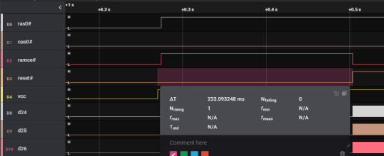
Another complication of using DRAM is the bus interface has been changed to allow much larger storage capacities without the physical chip package growing to absurd sizes. Instead of the chip accepting the entire address at once, it expects to be given a Row address (along with a Row Address Strobe [RAS#]) then a Column address (along with a Column Address Strobe [CAS#]), with myriad specific timing requirements for when each signal should be asserted and deasserted.
In short, DRAM is much more difficult to interface with compared to SRAM, so I've never really gotten around to it.
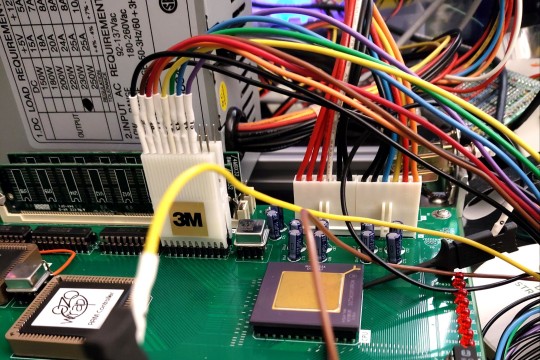
With one of the long term goals of this project being running a *nix operating system though, I'm going to need the larger memory that DRAM affords. So i made provision for a CPLD to serve as a dedicated DRAM controller on the Wrap030-ATX motherboard and added a couple 72-pin SIMM slots. In theory this setup should be able to support up to 256MB of RAM (if rare 128MB SIMMs should fall into my hands...).
So where do we turn when dealing with complicated timing with multiple modes and a bunch of I/O? Why, Finite State Machines, of course! That bit where the DRAM expects a row address for a little while, that's a state. And the following bit where the DRAM expects a column address is another state. And then another state to make sure the DRAM has enough time to write or fetch the data. The round it out with one last state to tell the CPU data is ready.
What about that weird refresh timing? Well, that's just few more states for the state machine. And then one last "idle" state that waits for a refresh timing counter to hit 0 or for the CPU to start a bus cycle. Laid out like that, the DRAM controller became a state machine with 7 or 8 states, a counter, and an address multiplexer.
The logic actually came together easier than expected. Not completely without bugs of course.
There's this note in the datasheets about startup initialization where the DRAM should not be accessed 200μs after power on, and there should be 8 refresh cycles before the first access. Initially I had built this entire sequence into my logic. It consumed a ton of resources and didn't really work right.
I realized that my reset circuit held the CPU in reset for longer than 200μs on power on, so I was guaranteed that first initialization time. So I removed that startup delay from my DRAM controller logic, and made a few tweaks to the state machine so it could do 8 back-to-back refresh cycles after reset.
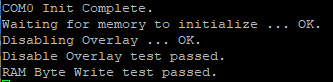
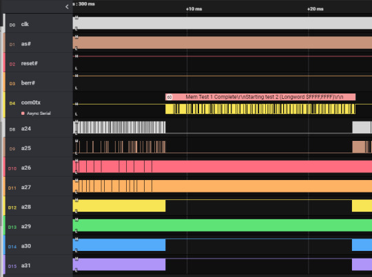
I was able to successfully write to DRAM and read that data back!
That much proved to be the easy part. The next steps were confirming DRAM accesses worked reliably, that I had the order of my byte select signals correct, that I could identify the amount of installed memory, and that all of the installed memory was working. These are programming problems, not logic problems, and I am not a strong programmer. On top of that, not only am I working with unproven DRAM logic, but I'm also using untested SIMMs that I had picked up from Computer Reset.
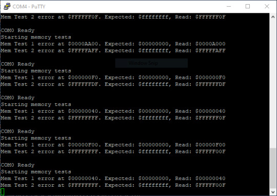
I quickly ran into errors, but was it a problem with my logic? A problem with my timing? A problem with the SIMMs?
I had a large back of 72-pin SIMMs, split fairly evenly between Fast Page Mode (FPM) and Extended Data Output (EDO) types. I tried them all. Some would pass the tests for nearly all addresses but fail at the end. Some seemed to have a stuck bit. Some were just plain bad and gave errors everywhere. It didn't really answer the question about whether my logic was bad, but results were consistent enough for me to think that maybe the logic might be ok.
And then finally I came across a pair of HP-branded 8MB EDO SIMMs that passed a simple write-read test without error ...
... right around the time my serial port stopped working. But the memory test was passing, and I could at least see the serial output on the logic analyzer.
The serial port problem was a bit setback. It had been working but suddenly wasn't. Clearly the UART itself was working, I just wasn't getting anything past the level shifter. Well that at least gave me a starting point of where to look. Sure enough, one of the 12V supply pins was not well soldered. Thankfully a quick fix.
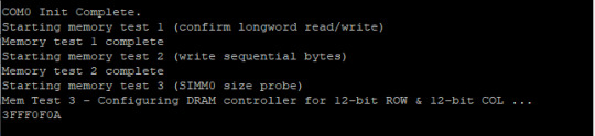
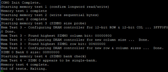
Back to testing memory, I started writing a program to identify the size of the installed SIMM and write a register I added to the DRAM controller to configure the specific geometry of the installed memory. See, DRAM has another lovely quirk — chips of the same size may have a different configuration of Row and Column sizes. For instance one chip may have a 9-bit Column and a 10-bit Row, but the next may have a 10-bit Column and a 9-bit Row, and both are the same size. If the DRAM controller just assumes 12-bit Row and Column (the largest supported by 72-pin SIMMs), then there will be gaps in the memory map that will need to be accounted for in software (using MMU, for example). If the DRAM controller knows the geometry of the installed memory, then it can present the memory to the CPU as one contiguous block of memory.
And that's where I found my next bug. The system would just hang when trying to write to that DRAM controller configuration register.
... because I had forgotten to complete that part of the state machine. The result was the state machine would end up in a state for writing to the configuration register, but then it couldn't get out of it. Once I added the missing condition to the state machine logic I was able to correctly identify the geometry and size for my installed memory!
Wow that was long. This has been the biggest, most involved step in the process of bringing up this computer yet. It turns out there are a lot of moving pieces that have to all work together to get the computer running code from ROM and reading/writing DRAM.
Now that I have my main memory working, I should be able to get some software running. I'm hoping to at least have BASIC running in time for VCFSW at the end of June.
#homebrew computing#vintage computing#motorola#mc68030#motorola 68k#assembly programming#motorola 68030#vcf#VCFSW#vcf southwest#verilog#Dynamic RAM#CPLD#troubleshooting#wrap030 atx
33 notes
·
View notes
Text
youtube
How to Download ModelSim Simulator for FREE! | Step by Step Guide in HINDI - [4 Min]
Welcome to our comprehensive tutorial on how to download ModelSim Simulator, the leading industry-standard digital simulation tool. In this step-by-step guide, we will walk you through the entire process, ensuring a hassle-free installation experience. ModelSim offers advanced simulation capabilities for digital designs, making it indispensable for hardware engineers, students, and enthusiasts alike.
In this video, we provide you with detailed instructions to download ModelSim Simulator effortlessly. Starting from checking the system requirements to ensuring optimal performance, we cover every essential aspect. We also discuss the licensing process and provide solutions to common installation errors that you may encounter. Our aim is to equip you with the knowledge and confidence to successfully install and utilize ModelSim Simulator in your projects.
Don't miss out on harnessing the power of ModelSim Simulator for your digital simulation needs. Watch this tutorial now and kickstart your journey towards efficient hardware design and verification!
🔔 Subscribe to our channel for more informative tutorials and updates! 🔔
Subscribe to "Learn And Grow Community"
YouTube : https://www.youtube.com/@LearnAndGrowCommunity
LinkedIn Group : linkedin.com/company/LearnAndGrowCommunity
Blog : https://LearnAndGrowCommunity.blogspot.com/
Facebook : https://www.facebook.com/JoinLearnAndGrowCommunity/
Twitter Handle : https://twitter.com/LNG_Community
DailyMotion : https://www.dailymotion.com/LearnAndGrowCommunity
Instagram Handle : https://www.instagram.com/LearnAndGrowCommunity/
Follow #LearnAndGrowCommunity
#ModelSimSimulator#DigitalSimulation#HardwareEngineering#InstallationGuide#Tutorial#SystemRequirements#SimulationSoftware#HardwareDesign#vhdltutorial#vhdl#vhdlprogramming#verilog#veriloghdl#verilogtutorial#fpga#simulationsoftware#howtodownload#Youtube
2 notes
·
View notes
Text
Как подготовиться к собеседованию в Samsung Advanced Computing Lab
Как подготовиться к собеседованию в Samsung Advanced Computing Lab
Я работаю проектировщиком аппаратного блока графического процессора в телефонах Samsung, в рамках совместного проекта с AMD. Сейчас наш менеджмент расширяет команду и поощряет инженеров распостранять информацию о новых позициях среди своих знакомых. Я решил написать это пост для более широкой аудитории, так как множество людей, способных пройти интервью на RTL или DV позицию – больше, чем…
View On WordPress
#GPU#RISC-V#RTL#Samsung#Samsung Advanced Computing Lab#SystemVerilog#Verilog#интервью#Харрис & Харрис
4 notes
·
View notes
Text
celebrating fall with fletcher's checksum
This post originally appeared on my website.
why are checksums useful for fpga development?
Checksum functions are useful for error detection and data integrity. With respect to FPGA architecture development, a checksum can ensure the system is able to retain its state. For example, an FPGA programmed to behave like an AND gate should not start to act like an OR gate due fluctuations in voltage or temperature. Such problems may be caught by computing the checksum of the bitstream before configuring the FPGA, operating the device in the lab, and then extracting the bitstream and re-computing the checksum to ensure it has not changed.
The last two FPGAs that I worked on-with Indiana University's SAIL-IN Lab and the QuickLogic Corporation-used a scan chain configuration interface which lent itself well to bitstream verification via checksum. The scan chain acts like a serial shift register, stringing together all the configuration chain flip-flops in the FPGA fabric. As the bitstream flows through the head of the scan chain, one bit at a time, its checksum may be computed; and later re-computed as it flows out of the tail. For context, imagine a small, thirty-two flop scan chain and the corresponding bitstream, 0xdeadbeef. On the way in, the Fletcher's (32-bit) checksum will be 0xf13b. If the post-configuration checksum does not match, the engineers would know that there is an issue with the FPGA architecture.
Fletcher's checksum also produces check bytes (or a "tag"), which can be appended to the end of the original data, such that the new checksum of the data and the check bytes is zero. For the example bitstream 0xdeadbeef, the resulting check bytes are 0xd2f1. And the checksum of 0xdeadbeefd2f1 is 0x0.
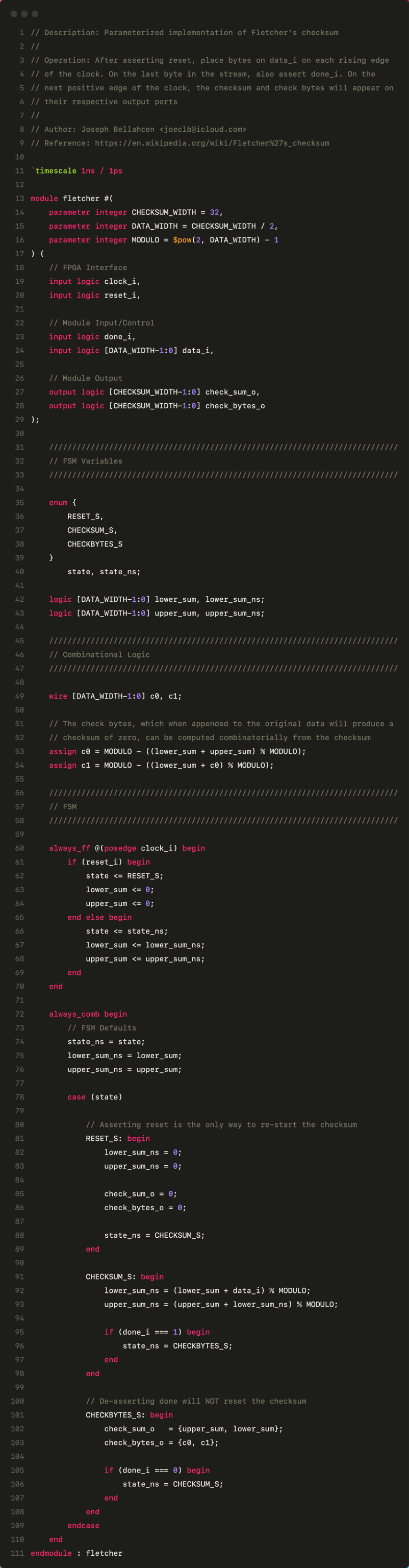
fletcher's checksum in systemverilog
Based mostly on the Wikipedia entry for Fletcher's checksum, I produced a parameterized, three-state module which computes the checksum and check bytes of a data stream. The SystemVerilog closesly follows the below psuedo-code. For the Fletcher-32 checksum, data arrives as 16-bit half-words.
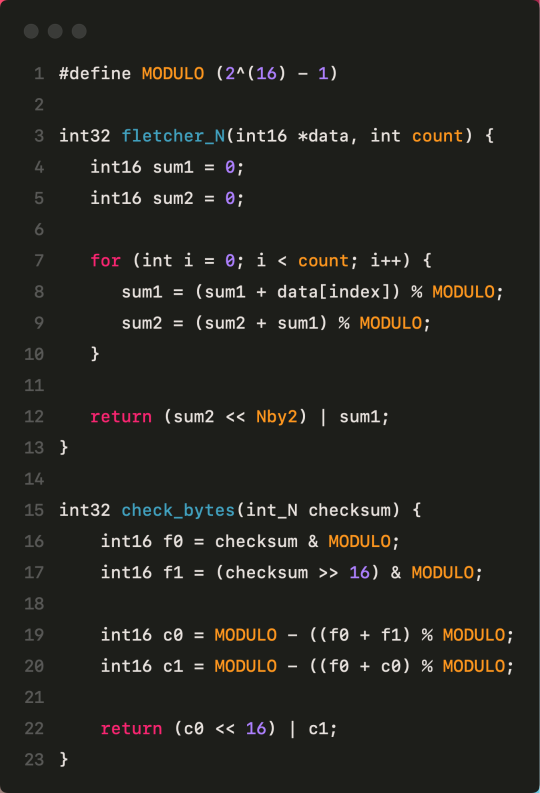
Eventually, I'd like to wrap it in a SPI interface and submit it to TinyTapeout, but for now here's the bare RTL. The most up-to-date code is also available on GitHub:
#engineering#computer engineering#fpga#verilog#systemverilog#hardware design#engineering student#studyblr
0 notes
Video
youtube
CSA Carry Select Adder 8 bit Code with Overflow in Verilog and VHDL with...
0 notes
Text
Johnny M - Flawless | 2022 Deep Progressive House Set
Johnny M – Flawless | 2022 Deep Progressive House Set
Digital Crate Digging Continues as we proceed and continue with this HumpDay Extravaganza, catch us broadcasting live and direct from our remote outpost out here off of I-20 in Atlanta!
The saga / struggle continues as life goes on as the toil and strife goes on; frontiers are local / national / international and intergalactic so somebody will understand a brotha!
We’re out here doing what we…
View On WordPress
#Abhishek#EvanDeNovellis#Fabreeka#housemusic#HumpDayExtravaganza#ODogDayParty#poetry#politics#Rockka#Saccao#Verilog
0 notes
Text
Catch me tryna figure out how to download extensions on eclipse
#I’ve only been using it for like. 2 months for Java#but I need an ide for verilog and I was told it could do this#it has occurred to me that I have zero clue how to then do this with the extension but that’s a later issue#issue one is I’ve lagged out eclipse and I’m hoping it’ll just sit for a few mins and fix itself#also Ik I could you VSC but I’m also scared of it. don’t know how it works and#importantly. when I tried to open extensions it went ahhh we can’t work and so I gave up immediately#one day I’ll spend sometime learning it
1 note
·
View note
Text
Innovative Arithmetic Core Projects for final years
Arithmetic Core projects are the true long-term direction in the evolution of mathematics today. Takeoff Projects is the spearhead of Flashpoint Projects, an arrowhead in the fight to bring about a new era of the computing prowess in the field of precision and speed standing at the Peak is digital processing power, and these projects are a combination of numerical exactness and computational effectiveness. Arithmetic Core is the key to creating the essential components of any technological device, including embedded systems and supercomputers as it focuses exhaustively on the fundamental arithmetic operations such as addition, subtraction, multiplication, and division. These projects are very meticulous in their where they aim to reach the peak performance while using the least resources and they are therefore applicable in industries like the industrial and infrastructure. Venture with us as we travel deeply into the centre of arithmetic calculation, where innovation and feature take the lead and unfold the advance of digital technology.

Based on customers' requests, our expert staff designs Arithmetic Cores for various products, ranging from embedded systems to high-performance computing. Using the cutting edge algorithms with the accurate design we achieve outstanding processing speed and precision. Our technology outperforms what is available in the market. Putting emphasis on reliability and versatility in mind, we develop the Arithmetic Core for the mission of corporations like the aerospace, telecommunications and the more. With the collaborative innovation which is fuelled mercilessly by the dedication projects, Takeoff projects are continuing to surprise boundary pushing definition of arithmetic computation in cutting edge technology, while transforming the technical aspects of digital space.
Latest:
A Lightweight True Random Number Generator for Root of Trust Applications
An Ultra-Efficient Approximate Multiplier With Error Compensation for Error-Resilient Applications
AxPPA Approximate Parallel Prefix Adders
Trendy:
Reversible Logic Based 1-bit Comparator using QCA
Fast Super singular Isogeny DiffieHellman and Key Encapsulation Using a Customized Pipelined Montgomery Multiplier
Implementation of Turbo Encoder and Decoder
An Optimized M-Term Karatsuba-Like Binary Polynomial Multiplier for Finite Field Arithmetic
Design of Approximate Radix-256 Booth Encoding for Error-Tolerant Computing
Standard:
Area Delay and Energy Efficient Multi-Operand Binary Tree Adder
Comparison of High Speed Adders Trade Area and Power
32-Bit Mac Unit Using Vedic Multiplier and Carry Save Adder
BCD Adder Designs Based on Three-Input XOR and Majority Gates
High Performance Filter Design using Adders and Multipliers
Finally, Takeoff Projects, being at the forefront of Arithmetic Core Projects, serves as a guide. By means of hard work, time consuming research, creative engineering, and unyielding persistence, we have created our book, which I am sure will become a great asset in the teaching of arithmetic. Our custom Arithmetic Core products, that have the marriage of efficiency, accuracy, and flexibility as its hallmarks, are absolutely primed to redefine this world changing industries. With a solid conviction that we have already arrived at the future of arithmetic processing and while we continue to push the boundaries of technological development, Takeoff Projects remains dedicated in their vision to transform our clients into the best-possible solution providers. Come along with us on this path unbounded by the sky, from where, powered by energy of imagination and a dedication to quality, we push to stay on the top.
#VLSI projects#Arithmetic Projects#ECE Projects#VLSI Projects#VLSI Projects for MTech#VLSI Projects using Verilog#VLSI Projects for MTech students#MTech VLSI Projects#IEEE VLSI Projects#VLSI Projects for Final Year ECE#VLSI Projects for ECE
0 notes
Text
VLSI Interview Questions and Answers for Freshers & Experienced | Maven Silicon
VLSI Interview Questions - VLSI Interview Questions and Answers for Freshers and Experienced candidates to help you to get ready for job interview, After preparing these VLSI, Systemverilog & Verilog Interview Questions, you will get placement easily, we recommend you to read VLSI interview questions before facing the real VLSI interview questions Freshers Experienced.
0 notes
Text
Wrap030-ATX First Code
This is a big step forward — Wrap030-ATX, my microATX form factor 68030-based homebrew computer, is running code from ROM. Externally, all it's doing is blinking an LED, but that LED is software-controlled, with a sizable delay loop between blinks to make it something that is human-visible.
Getting to this point took quite a bit of work after the free run tests. Nearly all of the logic on this project is in CPLDs. Of note here is the primary bus controller, which handles access timing, bus cycle termination, and a settings register.
For the computer to run code, it has to be able to read from ROM. Reading from ROM requires the bus controller to decode the CPU address, assert the ROM's Chip Enable (CE#) and Output Enable (OE#) signals, wait the appropriate length of time for the ROM to output stable data on the bus, and then assert the appropriate bus cycle termination signal for an 8-bit peripheral (DSACK0#).
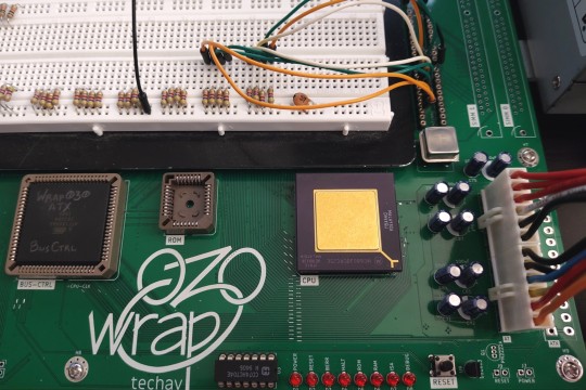
Once I had the minimal functionality for ROM access cycles, I was able to repeat the free run test, but this time with only the to 8 bits of the data bus (D[31:24]) pulled low.
Once I confirmed the ROM access cycle logic was working, I added the bus controller register access cycle logic. The bus controller has a single settings register that will control the Debug LED, startup ROM overlay, and ATX soft power. The CPU will need to be able to write to this register, and reading from it is helpful as well.
The bus controller logic is fully synchronous and managed by a state machine, so all that was needed to add the settings register was a couple new states for the state machine — one for read and one for write.
Put all that together, and we have a computer that can run the most basic of programs, with just a single LED for output.
The next thing I need to get working is a serial port. Everything that comes after this point will be a lot easier if I can output helpful debugging messages over serial.
#homebrew computing#motorola#mc68030#motorola 68k#verilog#cpld#motorola 68030#assembly programming#wrap030 atx#retro computing
26 notes
·
View notes
Link
Subscribe to "Learn And Grow Community"
YouTube : https://www.youtube.com/@LearnAndGrowCommunity
LinkedIn Group : https://www.linkedin.com/groups/7478922/
Blog : https://LearnAndGrowCommunity.blogspot.com/
Facebook : https://www.facebook.com/JoinLearnAndGrowCommunity/
Twitter Handle : https://twitter.com/LNG_Community
DailyMotion : https://www.dailymotion.com/LearnAndGrowCommunity
Instagram Handle : https://www.instagram.com/LearnAndGrowCommunity/
Follow #LearnAndGrowCommunity
#VHDL#VHDLDesign#BeginnersGuide#DigitalCircuitDesign#LearnVHDL#VHDLTutorial#VHDLBasics#hardwaredesign#FPGA#VerilogHDL#FPGAtools#DesignFlow#XilinxVivado#AlteraQuartusPrime#GHDL#Verilog#DigitalDesign#TimingAnalysis#FPGAdevelopment#LearnFPGA#FPGAdesignskills#FPGAbeginners#Career#Grow#LearnAndGrowCommunity#HDL#HardwareDescription#FSM#DesignVerification#DigitalElectronics
2 notes
·
View notes
Text
Что делать, когда выпускник топ-10 мирового вуза не может спроектировать блок сложения A+B
Что делать, когда выпускник топ-10 мирового вуза не может спроектировать блок сложения A+B
У меня был в свое время практикант из Стенфорда, от которого я получил инсайдерскую информацию, чему их там учат. Потом я интервьировал много студентов, и понял, что если человек не делает самостоятельных проектов в вузе, а просто плывет по течению программы как медуза, то будучи выброшенным на берег индустрии, он становится совершенно беспомощным.
Когда я вижу у недавнего выпускника в резюме…

View On WordPress
0 notes
Text
People who complain about plural teens being annoying about their headmates usually have no idea how annoying can be plurals with a job that they like.
Especially if different headmates have different jobs and help each other at that. It just does not stop.
#actuallyplural#nelke.txt#Oh you cannot handle fandom talk interspersed with plurality?#you will not survive five minutes of headmates conversing about Verilog
0 notes
Text
Irene twitter strip game but he just keeps having more layers inexplicably
1 note
·
View note
Last Seen Blogs

tokugou
this is where our story ends

yejapril
독일 신발

bloodnteeth
Blood & Teeth Collection

tollhaneul
Haneul the Erigom

potatoheadthewise
Geekgirl