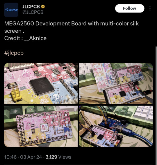
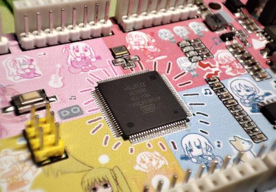
#pcb
Text
attention everyone: bocchi the pcb!


2K notes
·
View notes
Text

i wanted to draw yuyuko saigyouji! (❁´◡`❁)
18.10.23
#art#nonkiru art#touhou#touhou project#東方Project#東方#yuyuko saigyouji#西行寺幽々子#perfect cherry blossom#pcb#touhou 7#sorry for the like 2 people who saw this get deleted#spotted something that was coloured incorrectly!!
513 notes
·
View notes
Text

protect them at all costs
#ant man#quantumania#the quantum realm#ant man 3#ant man and the wasp quantumania#ant man quantumania#pcb#pink colored blob#quantum creatures#marvel#mcu#phase five#kang the conqueror
1K notes
·
View notes
Text
Bubble Bobble pcb
197 notes
·
View notes
Text


more toohoos
#touhou#touhou project#kanako yasaka#suwako moriya#youmu konpaku#yuyuko saigyouji#pcb#perfect cherry blossom#mountain of faith#mof
323 notes
·
View notes
Text

"I'll have my flowers, rotting princess!" / "I will loosen the seal, dog of the devil!"
#i thought the caption would look cooler but oh well#touhou#yuyuko saigyouji#sakuya izayoi#pcb#this work have been rotting in my ibis paint and i've only finaly finished it 3 months later mannn#it looks good though#this looks good#right guys#haha
64 notes
·
View notes
Text

#chen#chen yakumo#touhou#touhou project#touhou fanart#digital#fanart#perfect cherry blossom#touhou pcb#pcb
421 notes
·
View notes
Text

Message that appears when unlocking Phantasm difficulty in Perfect Cherry Blossom.
66 notes
·
View notes
Text
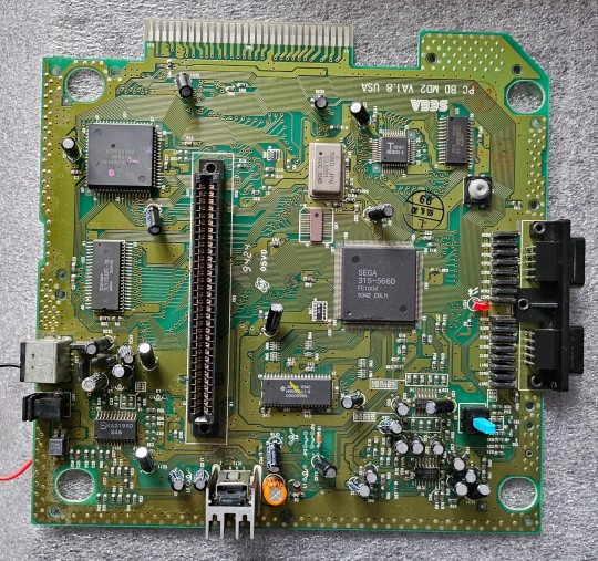
Sega Genesis 2.
Feliz año!
122 notes
·
View notes
Text


A poster series for all mainline Windows Touhou games.
This was my final project in college.
The theme was "adaptation". The project was about finding balance between what to translate and what to leave as is to preserve the themes of the original but still make it so the target audience understands them.
The titles use the Hungarian translation's titles and they were made in the style of '60's, '70's and '80's Hungarian posters and some elements were changed for understandability.
#touhou#2hu#eosd#pcb#in#pofv#mof#sa#ufo#td#ddc#lolk#hsifs#wbawc#um#this is the reason why I barely posted anything in the beginning of the year lol#these went through so many revisions#they're also months old at this point so I would change things about them but they're good enough#right also the Japanese kimono patterns I used are all symbolic#some more than others but still hgjdhs#each poster has a pattern
1K notes
·
View notes
Text


Flexible circuit boards manufacturing (JLCPCB, 2023)
Inkjet print head uses a fiducial camera for registering an FPC panel, and after alignment it prints graphics with UV-cureable epoxy in two passes
#jlcpcb#pcb#fpc#manufacturing#manufacture#factory#electronics#fiducial camera#camera#cv#opencv#computer vision
114 notes
·
View notes
Text
How a Computer Works - Part 3 (Miniaturization and Standardization)
For anyone just joining in, I'm writing a series of posts explaining perhaps haphazardly all there is to know about how a computer works, from the most basic fundamental circuitry components to whatever level of higher functionality I eventually get to. As explained in the first post on this subject, I am doing this just in pure text, so that if you are inclined you can straight up print these posts out or narrate them onto some audio tape or whatever and have full access to them should every computer in the world suddenly collapse into a pile of dust or something. Part 1 mainly covered the basic mechanical principles of circuitry and how to physically construct a logic gate. Part 2 covered logic gates in detail and how to use them to create a basic working architecture for a general purpose computer. Today we're going to be talking more about what you're looking at when you crack a machine open so you can make sense of all the important fiddly bits and have maybe a starting point on how to troubleshoot things with a multimeter or something.
Before getting into it though, I do have to shake my little donation can again and remind you that I do not know how I am going to get through the winter without becoming homeless, so if this is valuable to you, I'd appreciate some help.
Boards of Bread and Printed Circuits
With the things I've explained so far, you could totally build a computer right now, but it'd be a bit messy. You can totally buy resistors, transistors, capacitors, and diodes by the bagful for basically nothing, and cheap rolls of insulated wire, but there's all these long exposed pins to cut short and soldering things in mid-air is a messy nightmare and you'd just have this big tangle of wires in a bag or something that would almost certainly short out on you. So let's look into ways to organize stuff a little.
If you start playing around with electronics on your own, one of the first things you want to hook yourself up with besides raw components and wires is a breadboard or 12. And if you're watching people explain these things with visual aids, you'll also see a lot of them, so it's good to know exactly what they are and how they work. Your standard breadboard is a brick of plastic with a bunch of little holes in it. Incidentally, the name comes from how the first ones were literally just named after the wooden cutting boards for slicing bread people recycled to make them. Inside these holes there's some pinching bits of conductive metal which connect to each other in a particular way (pretty sure you can just see the strips that connect one if you pry the bottom off), so you can just jam a thing wire or prong into a hole, have it held in place, and make a connection to every other hole its connected to on the other side.
There is a ton of standardization to all of this. The holes should always be 0.1 inches apart () and split into two big grids. Everyone I've ever seen has 63 rows, each with 5 holes labeled A-E, a shallow channel through the middle of the board, and then another 5, F-J, and we generally have numbers printed every 5 rows. Down underneath, for any given row, the set of 5 pins on each side of the channel are connected. So, holes 1A, 1B, 1C, 1D, and 1E are all connected to each other, and nothing else. Holes 1F, 1G, 1H, 1I, and 1J are also connected to each other. There's no connection though between 1E and 1F, or 1A and 2A.
Most breadboards will also have a couple of "power rails" along the sides. These are just going to be labeled with a long red line and +, and a long blue or black line and -, and have holes in 2x5 blocks staggered out. With these, all 25 or 50 or whatever holes near the red + line connect with each other, and all the ones near the black line connect with each other. The gaps every 5 holes don't serve any purpose beyond looking different enough from the big grid so you hopefully don't mix it up and forget that these ones all connect down the length, and not in in little clumps across the width like everything else. The idea, for the sake of convention, is you plug a wire connected directly to the positive side of your battery or DC adapter or whatever into any red line hole, the negative side to any blue/black hole, and then tada, you can make a circuit just by plugging a wire in from red to a normal grid line, whatever bits you want span from that grid line to another, and eventually you connect the far end back anywhere on the black/blue line.
With a nice circuit board, there's also little snap-together pegs along the sides, and the power rails are just snapped on with those. So you can just kinda cut through the backing with a knife or some scissors, snap those off, connect multiple boards together without redundant power rails in the middle, and then just have these nice spare long lines of linked sockets. In the computer I'm building on these, I'm just using spare power rails for the bus. Oh and the big grooved channel down the middle also has a purpose. Bigger electronic components, like our good good friend the integrated circuit, are generally designed to be exactly wide enough (or more, but by a multiple of 0.1 inches) to straddle that groove as you plug their legs into the wires on either side, so they nicely fit into a breadboard, and there's a handy gap to slide something under and pry them off later on.
Typically though, you don't see breadboards inside a computer, or anything else. They're super handy for tinkering around and designing stuff, but for final builds, you want something more permanent. Usually, that's a printed circuit board, or PCB. This is pretty much what everyone's going to picture when they think about the guts of a computer. A big hard (usually) green board with a bunch of intricate lines, or "traces" running all over made of (usually) copper. And maybe with some metal ringed holes punched all the way through (they call those vias). These tend to look really complicated and maybe even a little magical, but they're honestly they're just pre-placed wires with a sense of style.
Most of the material of the board is insulated. The copper traces conduct real well, and manufacturers have done the math on just how close together they can be run without connecting to each other in places you don't want. The holes that go all the way through are for either plugging other bits in that tend to come with long legs you maybe want to keep intact, or just ways to run a trace through to the other side, where we often have traces on the back too to maximize our space. Most of what makes them look all cool and magical is how the traces run as close packed as possible to conserve space, and tend to only turn at 45 degree angles, which is just an artifact of how the machinery used to etch them out sued to be iffy about anything else.
So tada, you have all your wires pre-stuck to a nice sturdy board, and maybe even have labels printed right on there for where you solder all the various components to finish the thing. Oh and when you hear people talk about like, motherboards and daughterboards? The big main board you have for everything is a motherboard. Sometimes you need more than that, so you make smaller ones, and connect them up ether with some soldering or cartridge style with end-pins sliding snugly into sockets, and those we call daughterboards.
Integrated Circuits, or as they're also known, "chips"
The last thing you're likely to find if you crack open a computer, or just about any other electronic device that isn't super old or super super simple, are integrated circuits. Generally these are think black plastic bars that look like you'd maybe try to awkardly use them to spread cheese or peanutbutter on crackers in a prepacked snack or something, with rows of tiny little legs that running along either side. Kinda makes them look like little toy bugs or something. Sometimes they're square with pins along every edge, because sometimes you need a lot of pins. These are integrated circuits, or microchips, or just chips, and wow are they handy.
Sometime back in the 60s when people were really getting their heads around just how ridiculously small they could make electronic components and still have them work, we started to quite rapidly move towards a point where the big concern was no longer "can we shrink all this stuff down to a manageable size" and more "we are shrinking everything down to such an absurdly tiny size that we need to pack it all up in some kind of basically indestructible package, while still being able to interact with it."
So, yeah, we worked out a really solid standard there. I kinda wish I could find more on how it was set or what sort of plastic was used, but you take your absurdly shrunken down complex circuit for doing whatever. You run the teensiest tiniest wires you can out from it that thicken up at the ends into standard toothy prongs you can sink into a breadboard or a PCB with that standardized pin spacing, and you coat it all in this black plastic so firmly enveloping it that nothing can move around inside or get broken, hopefully.
And honestly, in my opinion, this is all TOO standardized. The only real visible difference between any two given integrated circuits is how many legs they have, and even those tend to come to some pretty standard numbers. They're always the same size shape and color, they all have the same convention of having a little indented notch on one side so you know which end is which, and they all seem to use just the worst ink in the world to print a block of numbers on the back with their manufacturer, date of assembly, a catalog number, and some other random stuff.
For real if there's any real comprehensive standard for what's printing on these, I can't for the life of me find it. All I know is, SOMEWHERE, you've got a 2 or 3 letter code for every manufacturer, a number for the chip, and a 4 digit date code with the last 2 digits of the year, and which week of that year it was. These three things can be in any order, other things can also be on there, probably with zero spacing, and usually printed in ink that wipes away like immediately or at least is only readable under really direct light, it sucks.
Once you know what a chip is though and look up the datasheet for it, you should have all sorts of handy info on what's inside, and just need to know what every leg is for. For that, you find which end has a notch in it, that's the left side, sometimes there's also a little dot in the lower left corner, and hopefully the label is printed in alignment with that. From there, the bottom left leg is pin 1, and then you count counterclockwise around the whole chip. You're basically always going to have positive and negative power pins, past that anything goes. You can cram a whole computer into a single chip, yo can have someone just put like 4 NAND gates on a chip for convenience, whatever.
OK, but how do they make them so small?
OK, so, mostly a circuit we're going to want to shrink down and put on a chip is just gonna be a big pile of logic gates, we can make our logic gates just using transistors, and we can make transistors just by chemically treating some silicon. So we just need SUPER flat sheets of treated silicon, along with some little strands of capacitive/resistive/insulating material here and there, and a few vertically oriented bits of conductive metal to pass signals up and down as we layer these together. Then we just need to etch them out, real real small and tight.
And we can do that etching at like, basically infinite resolution it turns out. It just so happens we have access to special acids that eat through the materials we need them to eat through, but that only work when they're being directly hit with fairly intense UV light. And a thing about light is when you have say, a big cut out pattern that you hold between a light and a surface, it casts a shadow on it... and the scaling of that shadow depends entirely on the distances between the light, the pattern, and the surface. So if you're super careful calibrating everything, you can etch a pattern into something at a scale where the main limiting factors become stuff like how many molecules thick things have to be to hold their shape. Seriously, they use electron microscopes to inspect builds because that's the level of tininess we have achieved.
So yeah, you etch your layers of various materials out with shadow masks and UV acid, you stack them up, you somehow align microscopic pins to hold them together and then you coat the whole mess in plastic forever. Tada. Anything you want in a little chip.
ROMs, maybe with various letters in front
So there's a bunch of standard generally useful things people put into ICs, but also with a computer you generally want some real bespoke stored values with a lookup table where you'll keep, say, a program to be run by feeding whatever's inside out to the bus line by line. For that we use a chip we call Read Only Memory, or ROM. Nothing super special there, just... hard wire in the values you need when you manufacture it. Manufacturing these chips though is kind of a lot, with the exacting calibrations and the acid and the clean rooms and all. Can't we have some sort of Programmable ROM? Well sure, just like build it so that all the values are 1, and build a special little thing that feeds more voltage through than it can handle and physically destroy the fuse for everything you don't want to be a 1.
OK that's still kind of a serious commitment. What if I want to reuse this later? Oh, so you want some sort of Erasable PROM? OK someone came up with a funky setting where you overload and blow out the fuses but then if you expose the guts of the chip to direct UV light through this little window, everything should reform back to 1. Just like, throw a sticker on there when you don't want to erase it. Well great, but can we maybe not have me desolder it and take it out to put under a lamp? Oh la de da! You need Electronically Erasable PROMs? EEPROMs? I guess we can make THAT work, somehow. They're still gonna be slow to write to though, can't have anything. I mean, not unless we invented like, flash memory. Which somehow does all this at speeds where you can use it for long term storage without it being a pain. So that's just kinda the thing we have now. Sorry I don't quite get the principles behind it enough to summarize. Something about floating components and needing less voltage or whatever. Apparently you sacrifice some read speed next to older options but hey, usable rewritable long term storage you just plug in, no jumping through extra hoops.
So OK. I think that's everything I can explain without biting the bullet and explaining ALUs and such. Well, there's keyboards (they're just buttons connecting input lines), monitors (these days, LEDs wired up in big grids), and mice (there's spokes in wheels that click X times or cameras checking the offset values of dust on your desk or whatnot).
Maybe throw me some money before we move on ?
CONTINUED IN PART 4
#computers#computer science#pcb#printed circuit board#integrated circuits#microchip#breadboards#education#electronics
54 notes
·
View notes
Photo

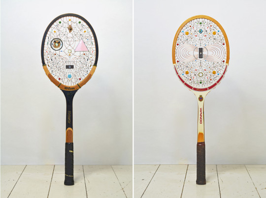
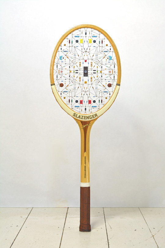

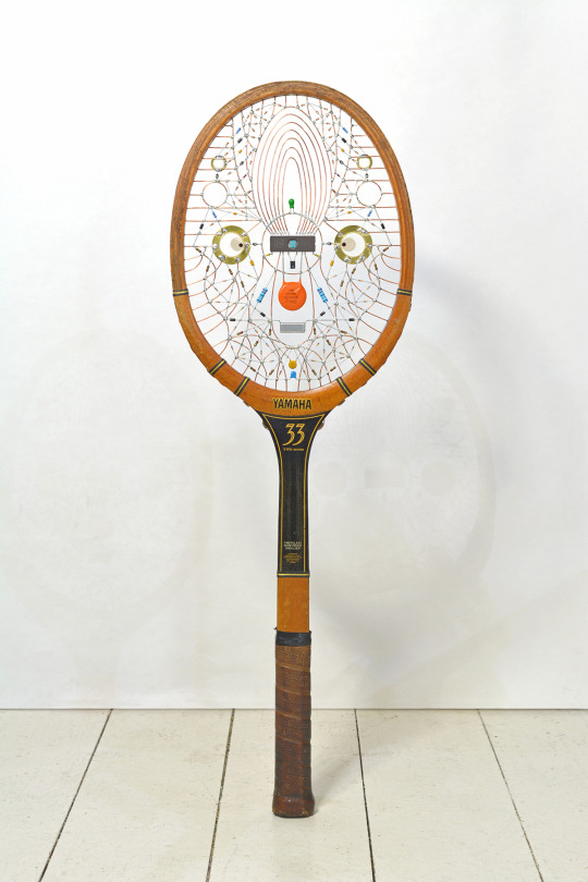

Leonardo Ulian - Contrived Object series
actually these could be functional circuits
cred: thisiscolossal.com/2020/06/electronic-rackets/
407 notes
·
View notes
Text


taoists and a couple of the sages
#touhou#my art#touhou project#hidden star in four seasons#hsifs#perfect cherry blossom#pcb#ten desires#toyosatomimi no miko#seiga kaku#yoshika miyako
91 notes
·
View notes
Text
145 notes
·
View notes
Last Seen Blogs

grandmamenu
Grandma Menu

w0wbagger
witty title

nicktups
cheap flowers by post aprilflorist.co.uk

iamnewhere
Random Thoughts I Have

bisexualincarnate
sour cream lobster