#best PCB manufacturing companies
Link
#PCB manufacturing companies in India#Fine-Line Circuits Limited#accredited publicly traded Indian PCB manufacturer#best PCB manufacturing companies
0 notes
Link
#cost-effective interconnect solutions company in San Jose California USA#quality printed circuit board manufacturers in San Jose California USA#PCB Manufacturers in San Jose California USA#good flex circuit manufacturer in San Jose California USA#printed circuit board manufacturers in San Jose California USA#rigid flex circuits manufacturers in San Jose California USA#best laptop circuits manufacturers in San Jose California USA#best autofocus camera circuit manufacturers in San Jose California USA#interconnect solutions company in San Jose California USA#best interconnect solutions company in San Jose California USA
0 notes
Text
Best PCB Production Company in India
PCB Power Market is a leading PCB production company in India. We offer high-quality, reliable printed circuit boards for a range of industries. Our PCB production services offer quick turnaround times and custom designs to meet your unique needs. We use state-of-the-art technology and have a team of experienced professionals to ensure the best possible results. Contact us today to learn more.
#PCB production#PCB production services#PCB production company#PCB production company in India#best PCB production company#PCB Power Market#PCB manufacturer
1 note
·
View note
Text
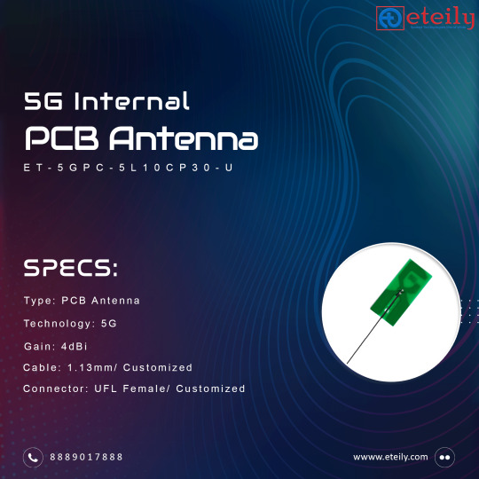
5G INTERNAL PCB ANTENNA
https://eteily.com/59-5g-internal-antenna
5G Internal Antenna
This internal antenna is specially designed for home and office use. It supports 5G network connectivity and works well with your existing router or modem. Our 5G internal antenna is the perfect companion to all your 5G devices.
#5G internal antenna#pcb antenna#5g antenna#radio frequency antenna#Best RF Solution Provider#RF Antenna Suppliers#Manufacturer of RF Antenna#rf antenna manufacturers in india#RF Antenna Manufacturer#RF Antenna Exporters#RF Antenna Latest Price#Wireless HF Antenna#RF Antenna Companies in India#Wholesaler of RF Antenna#RF Antenna Amplifier#RF Antenna Module#2.45 GHz Antenna Module#High Performance RF#Antennas for LoRa and Sigfox#Antennas for Cellular Gateways#Cellular External Antenna supplier#5G / LTE Cellular External Antenna manufacturer#Cellular 5G Antenna Solutions#Cellular Antenna Guide for 5G#LTE/5G Cellular External Antennas#Cellular Antennas 5G#Cellular Antennas LTE#Cellular Antennas CBRS#Cellular Antennas 2G#Cellular Antennas 3G
1 note
·
View note
Text
Manufacturing Process Of Brass Terminals
When it comes to the manufacturing process of brass terminals, it requires expertise, precision, and experience to deliver high-quality products that meet the needs of customers. Brass terminals are widely used in electrical and electronic applications because of their excellent conductivity, durability, and corrosion resistance. Therefore, it is essential to choose the best brass terminal manufacturer in India to ensure that you get the best products at a reasonable price.

The manufacturing process of brass terminals involves several steps, and each step requires careful attention to detail to produce a finished product that meets the exact specifications of the customers. Here is an overview of the manufacturing process of brass terminals:
Raw Material Selection:
The first step in the manufacturing process is to select the best quality brass raw material. The raw material should be of high purity, and its composition should be according to the required specifications. Therefore, it is crucial to choose the best brass terminal manufacturer in India to ensure that you get the best products at a reasonable price.
Cutting and Shaping:
After selecting the raw material, it is cut and shaped into the desired size and shape using precision tools and equipment.
Machining:
The next step is machining, which involves drilling, tapping, and turning the brass terminal to create the required features and dimensions.
Surface Treatment:
Once the machining is done, the brass terminal is cleaned and treated with a surface finish to enhance its appearance and provide protection against corrosion.
Quality Control:
The final step is quality control, which involves testing the brass terminal for its conductivity, durability, and other parameters to ensure that it meets the required standards.
If you are looking for the best brass terminal manufacturer in India, then you should choose a company that has a proven track record of delivering high-quality products and excellent customer service. A good manufacturer will have a well-equipped manufacturing facility, experienced and skilled workforce, and a robust quality control system to ensure that their products meet the highest standards.
At Excel Electricals, we are committed to providing our customers with the best quality brass terminals at a reasonable price. We have been in the business for over three decades, and our experience and expertise have made us one of the leading brass terminal manufacturers in India. We use the latest technology and equipment to manufacture our products and ensure that they meet the exact specifications of our customers.
In conclusion, the manufacturing process of brass terminals requires expertise, precision, and experience to deliver high-quality products that meet the needs of customers. Therefore, it is crucial to choose the best brass terminal manufacturer in India to ensure that you get the best products at a reasonable price. At Excel Electricals, we strive to deliver the best products and services to our customers and help them achieve their goals.
#business#manufacturer#electrical engineering#electrical products#electrical industry#electrical company#Best Brass Terminal Manufacturer in India#Best Electrical Panel Manufacturer in Vadodara#terminal blocks#current transformer#solar products#PCB connectors#DIN rails channels#2-rail junction box#3-rail junction box#4-rail junction box
1 note
·
View note
Text
Avalon Technologies Limited Is a Top EMS Industries In India
We Provide Services and Solutions Like:
Design
Engineering
NPI
Volume Production
Life Cycle Management
System Integration
PCB Assembly
Cable & Wire Harness
Sheet Metal
Aerospace Metal
Machining
Magnetics
Plastics
Supply Chain & Logistics
2 notes
·
View notes
Text
Doing your best with Performance and Good quality with PCB A particular-Conclusion Providers
Productiveness and high quality are important priorities in the creating industry, particularly regarding complicated operations like PCB age group. PCB one particular-cease guidance supplies a ideal way of capitalizing on productivity and top quality by giving organizations using a thorough treatment that mixes all steps of PCB creating under 1 roofing framework.
Among a number of main techniques PCB one-cease services improves performance is actually by smooth task management and collaboration. By partnering having a solitary dealer which provides design and style and elegance, developing, assemblage, and evaluating services, businesses remove the demand for several service provider partnerships and centralize business handle. This centralized approach boosts conversation, reduces information instances, and guarantees alignment across diverse stages of PCB manufacturing.
Furthermore, PCB an individual-cease support optimizes the production procedure by benefiting outstanding systems, digital goods, and constant processes to improve functionality and uniformity. From auto factor placing and soldering in assemblage to accuracy and reliability etching and drilling in developing, each time period of PCB creating is optimized for price, preciseness, and repeatability. This perfecting leads to a faster time-to-industry position, decreased generation service fees, and improved high quality administration techniques.
Furthermore, PCB One Stop Service good quality by implementing firm high quality managing approaches, inspection functions, and exams methods from the production approach. High-quality confidence professionals keep track of every element of PCB technology, from design customer feedback and components selection to last products testing and validation, producing particular the PCB meets enterprise specifications, consumer needs, and steadiness expectations. By embedding good quality into every one of the procedure, businesses can give great-high-quality PCBs that exceed client anticipations.
Additionally, PCB a single-cease assistance supplies scalability and suppleness allowing for altering venture requirements, creation quantities, and modification calls for. Whether it be a prototype improvement, small-establish manufacturing, or massive-range creating control, the company can get used to all the enterprise demands and provide customized possibilities that satisfy the recommended specs. This scalability permits businesses to handle business needs swiftly and successfully, taking advantage of working efficiency and resource work.
To summarize, PCB 1-quit service is important in enhancing efficiency and high quality in PCB production by giving organizations having a all-natural and included response that optimizes task supervision, producing methods, and good quality manage methods. By adopting a substantial treatment for PCB establishing, organizations can acquire functioning splendour, item stability, and customer service, finally traveling great outcomes and advancement available on the market.
related articles:
The Entire Good factors related to PCB A single-Cease Support
The Whole Advantages associated with PCB 1-Cease Assist
Top quality PCB One-Cease Services
0 notes
Text
Understanding Pack Develop Assemblage in Development
Box generate assemblage, also called method incorporation, can be a crucial phase through the entire manufacturing method where different variables and subassemblies are incorporated into the final items home or residences. This sophisticated development approach involves putting together electronic electronic digital elements, wiring, cable relationships, uncovers, and also other necessary elements in the pre-developed property to generate a determined item ready to do business with.
The package make assemblage strategy needs cautious prep, specific supplying, and physically challenging screening to make sure that the very best products or services fits superb specifications and profitable demands. Providers must carefully synchronize the set up of varied subcomponents, including PCBs, devices, cpus, and potential products, to guarantee correct fit, alignment, and functionality in the houses.
One of many crucial great things about box build assembly is that it streamlines the establishing treatment by consolidating many assemblage tactics inside the man or woman functioning. This technique diminishes the chance risk of faults, diminishes handling and touring expenses, and accelerates time-to-market for sophisticated electronic products. Furthermore, offer develop set up will allow suppliers to customize goods to meet specific client demands and design and style and magnificence options.
To obtain ideal results in package bargain produce assemblage, producers often make use of advanced automation engineering know-how, automated strategies, and top quality administration steps. These technological know-how boost set up accuracy and reliability and trustworthiness and balance, raise generation productivity, and improve uniformity inside the production approach. Great-good quality control research, which include beneficial checking, evaluation, and accreditation, are necessary to make sure the really prior services or merchandise meets company needs and consumer anticipations.
To assessment, container build design assumes a crucial role inside of the building of electric items, supplying an extensive solution for adding parts and subassemblies inside a carried out product. By boosting set up features, benefiting automation techniques, and looking after rigorous high quality manage actions, businesses can provide exceptional-excellent items that satisfy the calls for of today's intense industry location.
related articles:
Embracing Sustainability in Package Develop Set up
Being familiar with Box Build Assemblage in Manufacturing
Understanding Package Make Assemblage in Building
0 notes
Text
Nvidia AD103: A Powerful GPU Under The GeForce RTX 4070
Nvidia AD103
Nvidia has another RTX 4070 variant brewing this one uses a down-binned AD103 GPU from the RTX 4080 Super.
AD103 vs AD104
The Nvidia GeForce RTX 4070 ranks as one of the best graphics cards for gamers. Not surprisingly, TechPowerUp seemingly has confirmation that Nvidia released a new variant of the 4070 with harvested AD103 chips, which are normally used in the faster RTX 40-series models like the RTX 4070 Ti Super, RTX 4080 (now discontinued), and RTX 4080 Super. This is strictly business as usual, making use of every possible piece of silicon by turning off non-functional portions of the chip, and we previously reported on upcoming down-binned 40-series GPUs last month.
The RTX 4070 normally utilizes the smaller AD104 die. The silicon, a product of TSMC’s 4N Finfet manufacturing process, measures 294 mm² in die size and houses up to 35.8 billion transistors. Although 60 SMs (7,680 CUDA cores) are inside the AD104 silicon, the GeForce RTX 4070 only has 46 SMs (5,888 CUDA cores) enabled. The RTX 4070 Ti (also discontinued) used the fully enabled AD104 GPU, while the RTX 4070 Super has 56 SMs (Streaming Multiprocessors) enabled.
RTX 4080 AD103
AD103 has a die size of 379 mm² and 45.9 billion transistors, meaning it’s 29% larger and thus costs 29% more to manufacture (give or take). The full chip has 80 SMs (10,240 CUDA cores), which is what Nvidia puts in the RTX 4080 Super. AD103 also supports four 64-bit memory channels (256-bit total), which are used for the 4070 Ti Super and above, while the 4070 only needs three channels (192-bit total).
There shouldn’t be any noteworthy benefit to end users in getting an RTX 4070 based on a harvested AD103 chip. Rather, it’s Nvidia likely clearing out “faulty” chips that simply couldn’t meet the required specs for the higher-end Ada Lovelace models. This follows the usual pattern with prior GPU architectures, and Nvidia has likely been collecting AD103 chips that failed to meet the requirements for at least RTX 4070 Ti Super for over a year. Now, it has enough that it’s ready to sell them off as a late-cycle update to a lower tier product and with less than 60% of the SMs enabled, this should allow the use of nearly any remaining AD103 dies.
According to Tom’s Hardware, one TechPowerUp reader reported to the news outlet that the RTX 4070 (AD103) is already on the market. At least one known MSI model, the GeForce RTX 4070 Ventus 3X E 12G OC, is already using the AD103 die. TechPowerUp’s investigation shows that the new model is already supported in the latest Nvidia 552.22 drivers.
While the AD103 chips is physically larger than AD104, the PCB design, pin map, and package are apparently the same, allowing Nvidia and its board partners to swap between the GPUs as needed. Again, this was a premeditated design decision as Nvidia knew before the first Ada Lovelace GPUs rolled off the production line that it would inevitably have some chips that would require down-binning.
AD103 Nvidia
The Nvidia Blackwell RTX 50-series graphics cards will likely hit the retail market before the end of this year, starting with the highest performance models. Nvidia will want to clear out any existing Ada Lovelace silicon as quickly as possible between now and Blackwell’s launch, and recycling dies from one SKU to another represents a good way to do that. It wouldn’t be surprising to see Nvidia also release a variant of the RTX 4070 Super using AD103 all it would need is chips with at least 56 functional SMs.
Again, this silicon swap benefits Nvidia and its partners more than the consumer. The company is unlikely to lower the RTX 4070 (AD103) pricing or anything along those lines. Consumers will still receive an RTX 4070 with the same level of expected performance though GPU temperatures could be slightly lower thanks to all the “dead silicon” in the chips.
Minor elements of the new RTX 4070 model with a down-binned AD103 GPU are carried over from its higher-end cousin, while there may be minor modifications:
RTX 4070 AD103
Greater Die: Compared to the AD104 GPU that was originally included in the RTX 4070, the AD103 GPU has a larger die size. More transistors and possibly more processing power in theory may result from this.
Similar specifications: It most likely has a memory interface width of about 192 bits and 12GB of GDDR6X memory.
Potential Core Disparity: The AD103 model may include more Streaming Multiprocessors (SMs) than the original RTX 4070 (maybe 60, similar to the RTX 4070 Ti), however some SMs may be disabled to bring the performance closer to that of the original RTX 4070.
Standard capabilities: You may anticipate capabilities like hardware ray tracing and variable-rate shading along with support for DirectX 12 Ultimate.
Important Point: Because several cores have been disabled, this variation should perform similarly to the original RTX 4070. The primary distinction is in the GPU die underneath and maybe in the number of cores.
Read more on Govindhtech.com
0 notes
Text
Why epsilon is premier circuit assembly company in Gujarat?
Our Circuit Assembly matters as the first preference for all. In terms of the very fact that Gujarat is a leading electronics manufacturing destination in India. We have several years of experience as top circuit assembly company in Gujarat.
This company keeps an resolute policy for quality and ensures constant technological development. We has been a reliable business partner in the region and throughout. Be it small-scale prototypes or large-scale production runs, the company's proficient staff provides the steady, reliable results.
Being one of the leaders of circuit assembly company in Gujarat, We offers an unparalleled expertise of the circuit board assembly. The implementation of each process is ensured to be accurate and effective.
Epsilon electronics's Integrated Circuit Assembly is a complete provider of any of the three services. Printed circuit boards assembly, SMT manufacturing or comprehensive electronic contract manufacturing services. They have collect a strong reputation by offering leading technology and customer support.
You can consider us the best partner to help you with your circuit assembly company in Gujarat. You can visit now to know more about circuit assembly services that we provided.
0 notes
Text
Your leading PCB High Volume PCB Assembly supplier in China
With 15 years of experience and high efficiency in PCB assembly and manufacturing, HITECH CIRCUITS is the perfect source for Big Batch PCB assembly on a limited budget. If you are looking for a large PCBA assembly within your budget, we will be your ideal choice. HITECH CIRCUITS has more than 15 years of experience in the OEM/PCBA manufacturing and assembly of printed circuit boards, advanced production technology and equipment, professional engineers and purchasing team to provide our partners with personalized and complete process solutions. HITECH CIRCUITS’s supply chain services deliver supply chain innovation on demand. We offer a bold, yet proven service solution designed to grow market share and profit. Our innovative approach to managing the supply chain offers a complete business model that delivers the talent and transformative tools necessary to create predictability, reliability, and responsiveness across your entire supply chain. Our practitioners are passionate about supply chains. We have spent a generation understanding, refining and building the best in intelligent supply chains. We provide talent on-demand with expertise in data analytics and strategic technologies that can help you predict, plan and respond more effectively.
Some designs require assemblies in small volume, maybe just prototypes, while others require them in high volume. At SMT house, High Volume, Large Volume, or Big Batch PCB Assembly always refers to printed board assembly projects with quantities more than 5K pieces. HitechPCB has the capability to offer high volume PCB assembly services to meet your requirements of high-quality, competitive price, on-time delivery and smooth communication in any manner of full turnkey, consigned and partial turnkey.
Also, if your business is involved in applications that require high-volume PCB assembly, the company to contact is HitechPCB, because we’re a complete turnkey solution for printed circuit boards assembly, we are ideally suited for bulk PCB assembly orders. Our state-of-the-art equipments, large facility and wide range of highly-qualified experts give us the capability of high-volume PCB assembly of up to 9,000,000.
We are also the perfect source if you’re looking for large-order PCB assembly on a budget. Because of our high level of efficiency and more than 10 years of experience with printed circuit board manufacturing and electronics assembly, we offer large printed circuit board orders at surprisingly competitive prices compared to other PCB manufacturers or PCB assembly companies.
Our large order PCB assembly process starts with a tested and practiced set of workflow guidelines for every phase of the process, from pre-order PCB design consultation with professional veteran engineers to PCB fabrication, components sourcing, PCB assembly, PCBA testing, PCBA inspection, PCBA packing and shipping all under the auspices of a highly-skilled production staff. You can be confident that no matter how many circuit boards you order, you will enjoy fast service, low prices and extremely high quality.
With our excellent after-sales service, 24 sales and technical support team, quick response service, we will be your best Big Batch PCB assembly manufacturer inChina. A wide variety of highly qualified experts
Why choose Hitechpcba Big Batch PCB Assembly
Compared to our competitors, Hitechpcba offers large printed circuit board orders at very competitive prices. The risky big batch PCB assembly process begins with a set of tried and tested workflow guidelines. From ordering PCB design to component procurement, manufacturing, testing, assembly, inspection, shipping and packaging. This is all under the guidance of our highly skilled production staff.
No matter how many boards you order, you'll love the fast response service, low cost, and surprisingly high quality.
Whether you are seeking for product designer, electrical engineer, system integrator, manufacturer, or big batch PCB manufacturing and assembly, low cost big batch PCB housing, electronic assembly services, Hitech Circuits PCB Assembly team will be your perfect choice for big batch PCB assembly plant inChina.
Finding Reliable High Volume PCB Assembly Supplier?
When your design passed the prototyping verification after optimization, DFM and DFT check, it’s time to find a manufacturer or a supplier who has ability to perform high volume PCB manufacturing and assembly for you. HITECH CIRCUITS is a one-stop PCB solution provider, no matter which your design stage is located, we always can help in PCB manufacturing, assembly and design. With both design and manufacturing knowledge, we can feedback some suggestions to modify or change your design on the basis of cost-down without sacrificing the quality and performance. What’s more, if choosing our full turnkey PCB assembly service, we will be responsible of BOM sourcing to reduce your workload. Our approach to conducting high volume printed circuit board assembly is founded on a commitment to the highest possible quality, based on IPC standards and our inner quality control processes. In spirit of those high assembly standards, HITECH CIRCUITS developed excellent high-volume assembly capabilities and manufacturing processes relied on our advanced assembly lines in dust-free workshop.
What is big batch PCB assembly?
Big batch PCB assembly is an assembly process where you will assemble 10,000 or more PCBs in a specific period of time. The main processes you will use to assemble PCBs in large quantities are design for manufacturing and design for testing.
What are the advantages of using big batch PCB assembly? PCB assembly process
With applications in mind, big batch PCB assembly will provide you with numerous industrial and personal benefits. This is why electronic OEM prefer to use it in most of their applications.
The following are the main advantages of using mass printed circuit components:
Rapid design and prototyping process
Since you will be mass-producing or manufacturing printed circuit boards, you must assemble them uniformly. By simply creating a design and a prototype that works for each PCB, you can save a lot of time.
Short production cycle
Since the production process is fully automatic, you will also save time in the production of numerous PCBS. It all starts with the design and prototyping phase, which you'll do with the help of software and machines.
Production consistency
You will also have a very uniform production process because most of the details are predetermined before implementation. Once production begins, all manufacturing specifications will follow uniform specifications for all printed circuit boards.
Quality consistency
Since you will be producing all PCBs to similar specifications, you will automatically get consistent quality throughout the production process. In other words, you should rest easy knowing that you will have consistency across all printed boards.
First-class cost performance
This is the most convenient model for the cost of producing printed circuit boards because you can do everything very consistently. Here, you will buy all the materials in bulk and produce them in a short time using similar machines.
Improve the market's ability to time
You will be able to produce large number of printed circuit boards in a very short time, thus giving you the advantage in the market. In other words, you will have a steady supply of on-demand printed circuit boards, giving you the advantage in the market.
Do you have lead-free mass PCB assembly?
Yes, we care about the health of our users and the health of the environment. We are aware of the harmful or negative effects that lead emissions can have on users and the environment.That's why we eliminate lead from production materials. It is of great benefit to protect people's health and eliminate environmental pollution.
What is the testing protocol for mass PCB assembly?
As long as you have completed the process of producing printed circuit boards, you must ensure that they run well.
Existing testing protocols will help ensure that large volumes of PCBs are in perfect working condition.
Here are the main test protocols you can perform on a high volume printed circuit board:
Automated Optical Inspection (AOI)
You will use Automated Optical Inspection (AOI) tools to accurately and efficiently detect production errors in big batch PCB assembly. It has cameras and image-processing software that can identify assembly errors and relay information for further action. It is the best tool you will use for better error detection than visual inspection.
Solder Paste Inspection (SPI)
After you have finished printing with the paste printer, you must pass it through the paste inspector. The SPI machine has a camera and communication system equipment that can examine every detail of the solder paste.It compares these details to the Gerber file and reports any kind of inconsistency.
In-Circuit Test (ICT)
In-Circuit Test, you can use the most detailed test methods to check the quality and integrity of the PCB.Here, you will have to take personal initiative and use online testing software to check the quality of your PCB.You will use the machine to detect errors in the PCB for correction.
Functional Circuit Test
Here, you will use a computer with test pins or test probes to test the functional integrity of the PCB. You can tell if the board passes the test simply by comparing the results to the design specifications.
X-ray Examination
You will use X-ray inspection to detect welding problems on the PCB that are not visible to the human eye. Here, you do not have to cut through the circuit board to see the welding quality on the printed circuit board. You'll use X-ray inspection protocols to detect errors in components and soldering on circuit boards.
Do you have a custom mass PCB assembly?
Yes, we do customize mass printed circuit boards.
You can order the most unique types of printed circuit boards and we will produce them according to your needs.
We'll review your design, create a prototype, and then test how it works.
Once we confirm that it is working well according to the design details, we will proceed with the production process.
How does small batch PCB assembly compare to large batch PCB assembly?
On the production scale, you can choose between large batch PCB assembly or small batch PCB assembly.
Mass PCB assembly is the process by which you assemble 10,000 or more printed circuit boards.
It is a mass production or assembly system that can mass produce PCBs in a short period of time.
On the other hand, you can choose to assemble PCBs in small batches for small scale production or assembly of PCBs.
In other words, you will produce a very small number of printed circuit boards of 250 or less.
In large and small batch PCB assembly, the assembly process will remain the same.
In addition, you will use similar detection techniques for high - and small-lot PCB assemblies.
What are the main capabilities of mass PCB assembly?
Well, when you're looking for a good large volume PCB assembler, there are some special features.
This means that they must have the specific resources that you will use in the PCB assembly process.
The following are the main functions that must be available for mass PCB assembly.
Manufacturing capacity
It is important to have a manufacturer that can use both surface mount technology and through-hole technology.
You must find a manufacturer with sufficient knowledge and experience in surface mount technology and through-hole technology.
Fast turnaround time
You should also have a manufacturer that can produce large number of PCBs in a very short time.
In other words, you don't have to wait longer to get the printed circuit board you ordered.
Welding capacity
In this case, the key point you must pay close attention to is the ability to weld manually and by machine.Your manufacturer should be able to perform both hand and machine welds.
Quality compliance
You should also know that the quality of the printed circuit board is a top priority when it comes to durability and safety.
Here, your manufacturer must have the knowledge to read the list of materials and identify the right quality products.
Test method
You must also choose a manufacturer that has knowledge of all test machines and printed circuit boards.
In other words, after production, your supplier must test all printed boards accordingly before providing PCBs.
What are the applications of mass PCB assembly?
You will be mass-producing large volume PCB assemblies of different equipment at high rates.
If you want to enter the PCB production market, you must have knowledge of mass PCB assembly.
Here are some industries that require big batch PCB assembly.
The communications industry mass-produces communications equipment
Military or defense industry
Automobile industry
Aviation industry
You will be using big batch PCB assembly in an industry where big batch production, consistency, and consistency are important.
What is the cost of mass PCB assembly?
Well, the cost of mass-producing printed circuit boards is fairly affordable.
Here, you will apply economies of scale in the production process, thereby reducing the cost of producing PCBs.
In addition, other factors that affect cost such as quality and size will also play an important role.
You will spend more on high quality and larger PCB materials, increasing production costs.
Typically, the amount you will spend usually depends on the design specifications of your PCB.
How safe is the mass PCB assembly process?
Well, most of the manufacturing process for big batch PCBs is highly automated.
In other words, there was little human involvement other than the design and programming of the machine.
In addition, we eliminate any material that would suspend harm to the environment and users.
This makes mass PCB assembly one of the safest modes for producing printed circuit boards.
Do you provide both THT and SMT in big batch PCB assembly?
Yes, we have both through-hole technology and surface mount technology for PCB assembly.
These are the main manufacturing methods we use to produce high quality printed circuit boards.
You will choose among these manufacturing modes based on the design and application specifications.
Is there turnkey assembly for large volume PCB assembly?
Of course, our production system is capable of handling very large volumes of turnkey PCBs.
You'll find products that you can buy in bulk to meet your production needs.
Here, we will be responsible for every step of production from design, inspection, prototyping and assembly.
What is the turnaround time for mass PCB assembly?
You should rest easy knowing that your production specifications will be met as planned.
This includes time for all production specifications and you will accordingly meet all your market needs.
What are the quality certifications for mass PCB assembly?
As we mass-produce printed circuit boards, we also ensure consistent quality.
This means that you will get the highest quality printed circuit boards in large quantities at an affordable price.
Our quality meets and exceeds international quality standards, namely:
Comply with IPC quality standards such as IPC-WHMA-A-610 and IPC-CC-830B
ANSI/AHRI quality standards, such as ANSI/J-STD-001 -- Class II and III only
RoHS quality certification
UL quality standard
CE quality standard
What to consider when choosing big batch PCB assembly services?
You'll see the manufacturing capabilities of high-volume PCB assemblers.
Here are the main factors that you must pay close attention to:
Manufacturing and service capabilities
QC
Years of manufacturer experience
Customization capability
Turnaround time
Responsiveness and flexibility
Delivery service
Why is it difficult to scale up from prototype to high-volume assembly?
Scaling up from low-volume to high-volume PCB assembly can prove to be a difficult and painful process.
Here are the main reasons why this can pose a difficult challenge.
You must change design files and formats to meet new design requirements
You may also lack the correct type of machine for the new specification
You may also have to change components that will be tied to the PCB
You may also have to change the entire design to accommodate the new specifications
How do you simplify the transition from prototyping to high-volume PCB assembly?
Despite the difficulties, you should rest easy knowing that you can easily complete the process.
The best way is to choose the best prototype CM that can collaborate all the details accordingly.
It will help remove obstacles that can cause confusion and make the process difficult.
At Hitech Circuits, we will help you with the PCB fabrication and PCB assembly process.
Contact us today for all of your big batch PCB assembly needs.
Parts Quality Guarantee and Reliable Testing Methods
For verifying your turnkey orders, HITECH CIRCUITS would like to provide Prior PCB assembly service, which we will assemble 3-5pcs of your PCBs ahead of the main assembly production run, and ship these prior PCBAs to you for testing. This service is totally free of charge and only available for full turnkey PCB assembly orders in high volumes, which means HITECH CIRCUITS handling PCB fabrication, Components sourcing, and final assembly for your project. In this way, you can work with our assembly team to ensure that the finished product exactly meets your specifications every time. No one knows your design as well as you do, and so we offer prior Electronics Manufacturing assembly service as a guarantee that each and every board leaving our PCB and SMT facilities will meet your own personal standards in quality and performance. Of course, this is flexible threshold; we also would like to provide prior PCB assembly service for some smaller orders if they incorporate a high degree of complexity. Prior PCB assembly is especially popular among our customers who require IC programming services, since it allows for them to ensure that their source code will function as expected on the finished assembled boards, before their full order is assembled.
1 note
·
View note
Text
Addressing Common Myths and Misconceptions about Ceramic-Based PCB
Ceramic-based circuit boards are changing electronics with their great ability to handle heat and last a long time. But there are some myths and misconceptions about these ceramic based PCBs. Let's talk about what's really true about these special circuit boards.
Myth #1: Ceramic PCBs are too expensive for everyday use.
Fact: Sometimes, ceramic PCBs might seem more expensive upfront compared to regular FR4 boards. But that's not always true. If you need electronics that handle a lot of power or need to be super reliable, ceramic PCBs are worth it in the long run. They work better, so your devices last longer and have fewer problems with parts breaking.
Myth #2: Ceramic PCBs are too complex to manufacture.
Fact: Making ceramic PCBs needs special methods, but things have gotten easier with new advancements. Lots of good companies can make custom ceramic PCBs now, so they're available for more kinds of projects.
Top of Form
Myth #3: Ceramic PCBs are too fragile for real-world applications.
Fact: Ceramic is really strong and stable. Unlike FR4, which can get weak in extreme temperatures, ceramic PCBs are super durable and can handle tough environments easily.
Myth #4: Ceramic PCBs are only for high-powered electronics.
Fact: Ceramic base PCBs are great for powerful uses, but they're useful for more than that. They can handle really hot or really cold temperatures, so they're perfect for things like planes, medical devices, and factories. Plus, they're really good for stuff like radar and communication systems that need strong signals.
Ceramic based PCBs are a strong choice compared to regular ones. They're great at handling heat, lasting a long time, and working really well, which makes them a good pick for tough jobs. And now, it's getting easier to make them, so we can expect even better electronics in the future.
Don't believe the myths! Think about using ceramic PCBs for your project and discover how amazing this new technology can be.For best ceramic PCBs solutions contact to BSTCeramicPCB.
0 notes
Link
Cost-effective interconnect solutions company in San Jose, California, USA
#best interconnect solutions company in San Jose California USA#interconnect solutions company in San Jose California USA#best autofocus camera circuit manufacturers in San Jose California USA#best laptop circuits manufacturers in San Jose California USA#rigid flex circuits manufacturers in San Jose California USA#printed circuit board manufacturers in San Jose California USA#good flex circuit manufacturer in San Jose California USA#PCB Manufacturers in San Jose California USA#quality printed circuit board manufacturers in San Jose California USA#cost-effective interconnect solutions company in San Jose California USA
0 notes
Text
PCB Manufacturing Companies in Delhi: Shree Ram Electronics
PCB manufacturing companies in Delhi are pivotal for quality electronic production. At Shree Ram Electronics, a pioneer in the field, we excel in delivering top-notch PCB manufacturing services. Established under the visionary leadership of a woman entrepreneur, our ideology aligns with Make in India, contributing to the nation's growth. Our commitment to excellence, coupled with state-of-the-art technology and a skilled workforce, ensures unparalleled quality and precision in every PCB we produce. Trust us for your PCB manufacturing needs and experience innovation at its best.
0 notes
Text
The Role of PCB Test Fixtures in Waterloo and Montreal
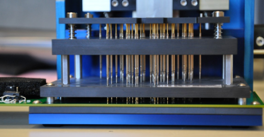
In the vibrant tech hubs of Waterloo and Montreal, where innovation and technology intersect, the demand for efficient electronics testing solutions is ever-present. PCB (Printed Circuit Board) test fixtures serve as indispensable tools for verifying the functionality and reliability of electronic components and assemblies. Let's delve into how PCB Test Fixture Waterloo and PCB Test Fixture Montreal play a crucial role in streamlining testing processes and driving technological advancement in these dynamic cities.
A PCB Test Fixture Waterloo, also known as a test jig or test rig, is a specialized tool designed to facilitate the testing of electronic circuits, assemblies, and devices. It consists of a custom-designed interface that securely holds the PCB in place and provides access to test points, connectors, and components for electrical testing.
PCB Test Fixture Waterloo are engineered to accommodate a wide range of PCB designs and configurations, from simple single-layer boards to complex multi-layer assemblies. They are essential for conducting functional tests, continuity checks, and performance evaluations to ensure the quality and reliability of electronic products before they reach the market.
The integration of advanced technologies such as automated test equipment (ATE), boundary scan testing, and in-circuit testing (ICT) further enhances the capabilities of PCB Test Fixture Waterloo, enabling faster and more comprehensive testing procedures.
In Waterloo, renowned for its vibrant tech ecosystem and world-class research institutions, PCB Test Fixture Waterloo play a pivotal role in accelerating product development cycles and driving innovation. Local companies and startups leverage these fixtures to validate prototypes, refine designs, and conduct rigorous testing to meet stringent quality standards.
With access to cutting-edge technologies and expertise in electronics design and manufacturing, PCB Test Fixture Montreal providers offer tailored solutions to address the diverse needs of clients across industries. Whether it's testing automotive electronics, medical devices, telecommunications equipment, or consumer electronics, these fixtures enable companies to achieve faster time-to-market and maintain a competitive edge in their respective markets.
In Montreal, a hub of technological excellence and innovation, PCB Test Fixture Montreal play an integral role in supporting the city's thriving aerospace, automotive, and electronics industries. Local companies and research institutions rely on these fixtures to validate designs, conduct reliability testing, and ensure compliance with industry regulations and standards.
PCB Test Fixture Montreal leverage their expertise in electronics engineering and manufacturing to deliver high-quality, reliable solutions tailored to the unique requirements of each client. Whether it's testing avionics systems, power electronics, or IoT devices, these fixtures enable companies to achieve optimal performance and reliability in their products.
Collaboration between PCB Test Fixture Waterloo and PCB Test Fixture Montreal, technology companies, and academic institutions drives innovation and technological advancement. By sharing knowledge, resources, and best practices, stakeholders in these cities contribute to the development of cutting-edge testing solutions that push the boundaries of what's possible in electronics design and manufacturing.
PCB Test Fixture Waterloo and PCB Test Fixture Montreal play a critical role in the electronics testing process, enabling companies in Waterloo and Montreal to validate designs, ensure quality, and drive technological advancement. By leveraging advanced technologies and expertise, these fixtures streamline testing procedures, accelerate product development cycles, and maintain the high standards of quality and reliability expected in today's competitive markets. As Waterloo and Montreal continue to thrive as centers of innovation and excellence, PCB Test Fixture Waterloo and PCB Test Fixture Montreal will remain essential tools for advancing technology and driving progress across industries.
0 notes
Text

What is Rogers PCB?
Rogers PCB is a type of printed circuit board (PCB) material made from a combination of epoxy and ceramic. It is well known for its high dielectric constant, low loss tangent, and high thermal conductivity, making it an ideal material for high-frequency applications. It is used in a wide range of electronics, such as:
5G Station
Cellular Base Station Antennas and Power Amplifiers
Automotive Radar and Sensors
Microwave point to point (P2P) links
LNB’s for Direct Broadcast Satellites
Microwave equipment of all kinds.
RF Identification (RFID) Tags
Rogers PCB is produced using the raw materials of the Rogers Company. Rogers company manufactures the laminate materials that are often used for manufacturing circuit boards. The Rogers PCB is a type of high-frequency PCB board, quite different from the traditional PCB board materials, epoxy resin. It uses the ceramic base as the material of high frequency. The major advantage of Rogers PCB is the temperature stability and superior dielectric constant.
Rogers PCB has a major application in high-speed electronic designs, radio frequency applications, and commercial microwaves. The low water absorption capacity of this Rogers PCB is ideal for the application of high humidity. Other Rogers PCB applications include RF identification tags, power amplifiers, automotive radar, sensors, etc.
Rogers PCB fabrication needs in-depth research on high-frequency PCB. HITECHPCB is a Rogers PCB manufacturer and has a deep understanding of the performance of Rogers PCB material. For example, Rogers PCB laminates and Rogers PCB dielectric constant in Rogers PCB material properties Rogers PCB is a high-frequency PCB material model produced by Rogers company, different from the conventional FR-4 PCB material. There is no epoxy resin in the Rogers PCB material, and Rogers ceramic PCB is used as the High-frequency PCB material. Absorption of Rogers PCB, it can be used as an ideal choice for application ns in high humidity environments, providing customers in the high-frequency PCB industry with the highest quality.
Difference Between Rogers Materials and FR-4 Materials
By combining Rogers PCB layers with FR-4 layers, we can achieve reduced cost and maximum performance compared to if we used only Rogers layers. Thus, this process should use Rogers PCB cores instead of prepregs for this process.
FR-4 stack up with 6 layers is shown below. Because prepreg is less expensive than cores, it is placed on the outside to minimize cost. A foil build is often referred to as this.
Rogers layers are required on the outside layers, but the core is usually found on the layers that need them. Below is an example with 6 layers but with 3 cores instead of 2. This configuration is sometimes called a "core build" or "cap construction" board. Rogers PCB is a high-frequency circuit board that has ceramic laminates and reinforced hydrocarbon. A Rogers PCB may be made from cores and prepregs, but most often, the top two copper layers are carried on the core, while the rest of the board is made from standard FR-4 to reduce the cost. The PCB materials absorb the signal, due to which it has less signal loss compared to that of FR-4. At higher frequencies, the signal loss is greater in FR-4 materials. This is also the signal length and design dependent.
High-Frequency
PCB with FR-4 materials is preferred due to their low cost, reliability, and well-understood electrical and mechanical properties. They are used in various applications ranging from microwave designs to audio circuits. Unfortunately, FR-4 printed circuit boards are not suitable for high-frequency applications. Rogers created the most well-known high-frequency-special laminates. Its materials have a constant dielectric reduction of close to 20% when compared to FR-4 printed circuit boards.
The best way to determine whether your project will benefit from high-frequency laminates is to assess electrical and mechanical requirements. If you find both variations are too broad, Rogers PCB material is a better option.
Dissipation
The material used is most important when producing printed circuit boards, though it may require a high cost. However, it is not the only issue that knows the content value when it comes to the loss factor or Df. FR-4 printed circuit boards will be affected or reduced. The losses are greater when compared to printed circuit boards made from Rogers materials.
In other words, when compared to Rogers PCB, FR-4 materials have a higher dissipation factor, especially at high frequencies. Typical values for FR-4 printed circuit boards are around 0.020 and close to 0.004 for Rogers boards. Dissipation of FR-4 materials increases with frequency. High-frequency laminates primarily have a frequency-dependent stable dissipation characteristic.
The signal loss is minimized with the lower dissipation factor in FR-4. Also, the automated assembly process and the processing of FR-4 materials make them easier in the assembly and manufacturing process.
Impedance Stability
Impedance is the measure of the current opposition when applying voltage. In many design applications, the stable impedance is essential and is an area where the materials like Rogers and FR-4 are applied.
FR-4, despite its low cost, is prone to high variations in the dielectric constant with the change in temperature across the length and width of the substrate. In terms of impedance stability, Rogers' material has a wider range of dielectric constants than FR-4 content.
High-frequency laminates are preferable for circuits that require little variation over wide temperature ranges. In this case, you may need to use printed circuit boards made of Rogers materials rather than FR-4 materials, especially if most of your operations involve working in high-temperature environments.
Dielectric Constant
The dielectric constant of any material measures a substance's ability to store some electrical energy across an electrical field. When it comes to dielectric constant, FR-4 has a dielectric constant of about 4.5, which is much lower than Roger's material, which has a dielectric constant of about 6.15 to 11.
The dielectric constant of FR-4 is comparatively higher than that of plastic materials. Using FR-4 materials can save at least 25% of PCB made from such materials. Other factors that make FR-4 articles available include their lightweight, moisture resistance, and high dielectric strength. Even though the Rogers PCB has a higher dielectric than FR-4, you can go with FR-4. FR-4 and Rogers 4350b and 4350 are similar manufacturing processes, although FR-4 stores electrical energy effectively.
Thus, PCB with higher dialect trends breaks easier when subjected to intense electric fields.
0 notes
Last Seen Blogs

maayavalan
Untitled

hoista
DigiCrypt

dinxh
ʙʀᴏᴋᴇɴ ᴡɪɴɢs

tierkhaos
Rosen-Kranz-Zwei

eltenshi
EL TENSHI