Last Seen Blogs

chandakgroup1
Chandak Group

beebboppop
booker


roleplayingspinosaurus
Archived

zapatterson
I know you now, I know I can trust you
Text
What is Heavy Copper PCB or Thick Copper PCB?
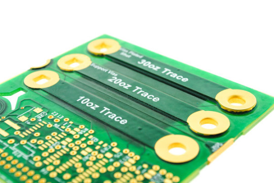
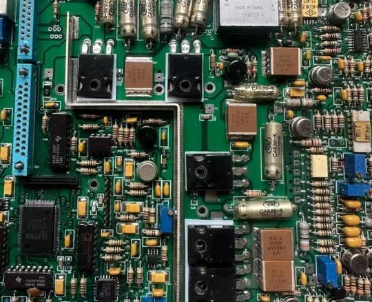
In high-power applications, managing ultra-high thermal loads and high-power currents is crucial. Standard PCBs typically have copper thicknesses ranging from 1oz to 3oz. However, in scenarios requiring robust current management and thermal dissipation, Heavy Copper PCBs, also known as Thick Copper PCBs, come into play. These boards have finished copper weights between 4oz and 10oz, with some super thick copper PCBs reaching 20oz to 200oz per square foot. The increased copper thickness enables these PCBs to handle high current outputs and optimize thermal management, crucial for electronics applications where temperature control is paramount to avoid performance degradation and premature failure.
Additionally, thick copper layers allow for large PCB cross-sections, which are ideal for high current loads, and facilitate heat dissipation. These PCBs also enable the integration of finely laid out structures on the outer layers with thick copper layers on the inner layers, providing a versatile solution for various design requirements.
Construction of Heavy Copper PCB
Manufacturing thick copper PCBs involves a combination of etching and electroplating processes, similar to standard PCBs. However, special techniques are required to ensure that trace sidewalls and undercuts meet the standards for thick copper features. Some of the main challenges in manufacturing thick copper PCBs include the need to remove a significant amount of copper during etching, increased etching costs, and the difficulty in manufacturing thin traces and ensuring the evenness of thick traces.
How to Make Thick Copper PCB?
The manufacturing process for thick copper PCBs involves several key steps to ensure the even thickness of the copper layers. These steps include etching inner layer traces on each layer of the inner core material, designing pads with uniform spacing and positioning, and using appropriate methods for burying copper in the prepreg. Common processes for thick copper PCBs include inserting thick copper bars into the circuit board, using laminate deposition with a thick base copper, and burying copper in the prepreg using laser cutting.
Advantages of Heavy Copper PCBs
Heavy Copper PCBs offer several advantages over standard PCBs:
Excellent high heat resistance: Heavy Copper PCBs can withstand high temperatures, making them ideal for high-power applications.
Improved current carrying capacity: The increased copper thickness allows Heavy Copper PCBs to carry larger currents with the same line width.
Reduced complex wiring: Heavy Copper PCBs can simplify complex wiring configurations, leading to more efficient designs.
Compression of board size: Heavy Copper PCBs allow for the integration of multiple copper weights on the same PCB, reducing the overall size of the end-use product.
Enhanced mechanical strength: The use of thick copper in PCBs improves the mechanical strength of the board, particularly in areas such as PCB connector areas and plated through holes (PTH).
Improved thermal management: Heavy Copper PCBs facilitate better heat dissipation, which is crucial for maintaining the performance and longevity of electronic components.
Ordinary PCB vs. Heavy Copper PCB
The main differences between standard PCBs and Heavy Copper PCBs lie in the manufacturing process and the copper weight. Standard PCBs are made through processes such as etching, hole drilling, and electroplating, while Heavy Copper PCBs require finer differential pair etching and step plating processes to ensure trace quality. Additionally, the copper content per square foot of a standard PCB is between 1oz and 3oz, whereas for Heavy Copper PCBs, the copper content exceeds 3oz.
Difference between Copper PCB and Heavy Copper PCB
Copper PCBs and Heavy Copper PCBs serve different purposes, with the main distinction being the thickness of the copper foil. Copper PCBs refer to PCBs with a copper substrate, which helps dissipate heat and prolong the life of components. On the other hand, Heavy Copper PCBs have a copper thickness exceeding 3oz and are used for their high current-carrying capacity.
Characteristics of Heavy Copper PCBs
Heavy Copper PCBs offer several unique features:
Ultra-high mechanical strength: Thick copper layers enhance the mechanical strength of the PCB, making it more resistant to weather and external stresses.
Excellent weather resistance: Heavy Copper PCBs can withstand extreme temperatures and harsh environmental conditions, ensuring the stability of the circuit transmission signal.
Thermal management: Thick copper layers improve heat dissipation, crucial for modern, high-density PCBs with high current loads.
Excellent current conduction: Heavy Copper PCBs provide excellent conductivity, facilitating the transmission of electricity between various components.
Diversity: Heavy Copper PCBs support various conductive and substrate materials, production processes, and application fields, making them versatile for different design requirements.
In conclusion, Heavy Copper PCBs play a crucial role in high-power applications where robust current management and thermal dissipation are essential. Their unique construction and characteristics make them ideal for applications requiring high heat resistance, excellent current carrying capacity, and improved thermal management.
High quality PCB manufacturer from China
0 notes