
Last Seen Blogs

snhboutique
SNH Boutique

unicornopornopyro
Untitled

gtwtits
they [redacted] in that cactus ring!!

timmytoms-moved
MOVED

sizzlingmoonsaturnclam-blog
artist at heart
Text
Latest trends in PCBs
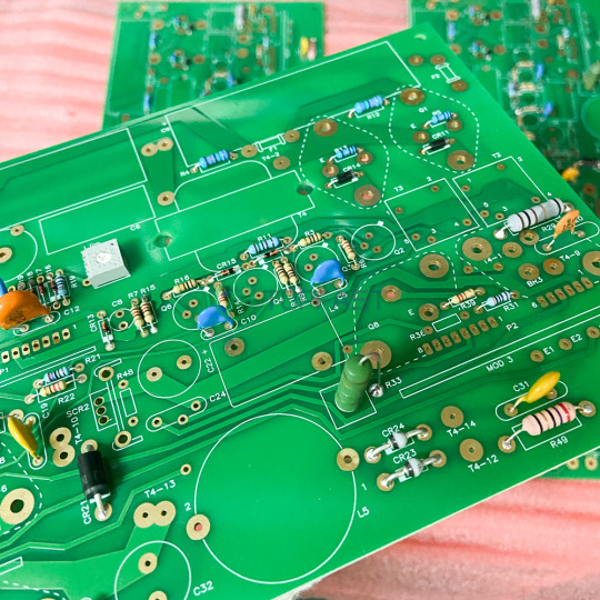
Today's electronic devices play an increasingly important role in our daily lives, from smartphones to automotive control systems to medical equipment and industrial robots. At the heart of these devices is the Printed Circuit Board (PCB), which is the cornerstone of modern electronics manufacturing. In this article, we will dive into some key concepts and latest trends in PCBs.
Basic knowledge of PCB:
A PCB is a substrate that supports and connects electronic components, usually made of insulating material coated with a layer of conductive copper. They provide the support structure for electronic components while providing the electrical connections that allow electronic devices to function properly.
Different types of PCB:
There are many types of PCBs, including single-layer boards, double-layer boards, and multi-layer boards. Single-layer boards consist of a layer of insulating material and a layer of conductive copper, and are suitable for simple circuits. Double-layer boards have a conductive copper layer between two layers of insulating material and are suitable for slightly more complex circuits. Multilayer boards have multiple insulating and conductive layers and are suitable for highly complex electronic devices such as smartphones and computer motherboards.
PCB design process:
PCB design is a complex process that includes circuit design, layout, routing, component placement and final manufacturing file generation. Modern PCB design often uses CAD (Computer Aided Design) tools for greater efficiency and accuracy.
PCB manufacturing technology:
The manufacturing process of PCB includes steps such as chemical etching, etching, drilling, printing, assembly and soldering. As technology develops, PCB manufacturing becomes more sophisticated, allowing for smaller, lighter, and more powerful electronic devices.
Latest trends and future outlook:
The PCB field is constantly evolving, with many new challenges and opportunities. Some of the latest trends include:
High Density Interconnect (HDI) PCB: As electronic devices become more and more miniaturized, HDI PCBs are becoming more and more important. They have more layers and smaller traces/spacing to accommodate more components and functionality.
Flexible PCB: Flexible PCB allows electronic devices to be more flexible, suitable for curved surfaces and foldable devices. This is a key component in products like wearable technology and foldable phones.
Environmentally Friendly PCBs: Environmental awareness is driving improvements in the PCB manufacturing process to reduce the use of waste and hazardous materials.
In the future, we can look forward to the continuous evolution of PCB technology, opening up broader possibilities for smarter and more efficient electronic devices.
PCBs are an integral part of modern electronics manufacturing, and their design and manufacturing processes are constantly evolving to meet growing demands. A thorough understanding of PCB basics and latest trends will help you achieve greater success in the electronics field. If you have more questions about PCB or electronics manufacturing or would like to explore this topic further, please feel free to contact me.+8613929576884
0 notes
Text
Fast data rates on FR4 board material and connectors have become increasingly important in today's technological landscape. FR4, a widely used substrate material in printed circuit boards (PCBs), offers excellent electrical and mechanical properties. However, as data rates continue to rise, the limitations of FR4 in terms of signal integrity and transmission losses become more apparent. To address this, designers and engineers are exploring various techniques to optimize FR4 board performance.
When it comes to maximizing bandwidth and speed using PCB traces, several factors come into play. PCB traces refer to the conductive paths on a printed circuit board that connect various components. To achieve higher bandwidth and speed, designers need to consider trace width, length, impedance, and signal integrity.
One crucial aspect is trace width. A wider trace allows for better current flow and reduces resistance, enabling higher data transfer rates. By carefully selecting the appropriate trace width based on the current requirements, designers can optimize signal integrity and minimize signal degradation.
Impedance matching is also critical for maximizing bandwidth. Impedance refers to the resistance to the flow of alternating current in a trace. By ensuring that the impedance of the trace matches the impedance of the source and the load, designers can prevent signal reflections and maintain signal integrity throughout the transmission line.
When it comes to maximizing bandwidth and speed using PCB traces, utilizing high-frequency signals such as Up to 14.0 GHz / 28 Gbps poses unique challenges. PCB traces act as transmission lines, carrying signals between components on a printed circuit board. To achieve maximum bandwidth and speed, several factors need to be considered.
Firstly, the choice of materials for the PCB is crucial. High-speed signals demand low dielectric constant (Dk) materials with low loss tangent (Df). Materials like PTFE (Polytetrafluoroethylene) or other specialized laminates with low Dk and Df values are commonly used to minimize signal degradation and maintain signal integrity.
Lastly, it is essential to consider the manufacturing capabilities and limitations of the PCB fabrication process. Higher frequencies require tighter tolerances and more precise manufacturing techniques. Collaborating with experienced PCB manufacturers who specialize in high-speed designs is crucial to ensure the best possible performance.
In conclusion, maximizing bandwidth and speed using PCB traces for signals Up to 14.0 GHz / 28 Gbps requires careful consideration of materials, trace design, impedance matching, EMI reduction, trace length, and manufacturing capabilities. By addressing these factors, engineers can optimize signal integrity and achieve the desired performance in high-speed PCB designs.
0 notes
Text
See how a PCB amazing!
1 note
·
View note
Text

We are a 20 years PCB&PCBA factory.
4 notes
·
View notes