#Digital Integrated Circuit Temperature Sensor Market
Text
Digital Integrated Circuit Temperature Sensor Market

0 notes
Text
Digital Integrated Circuit Temperature Sensor Market Future Aspect Analysis and Current Trends by 2017 to 2032
A digital integrated circuit temperature sensor is a type of sensor that is built into an integrated circuit and is used to measure the temperature of the surrounding environment. It uses various physical phenomena such as the temperature coefficient of resistance or the voltage-temperature characteristics of a diode to measure temperature. The output of the sensor is in the form of a digital signal that can be read and processed by a microcontroller or other digital circuitry.
Digital integrated circuit temperature sensors are widely used in a variety of applications, including temperature monitoring and control systems, environmental monitoring, and consumer electronics. They are often used in conjunction with microcontrollers or other digital circuitry to provide accurate and reliable temperature measurements in real-time.
This report provides a wide range of research and data that will assist users in understanding niches and focusing on key market channels in the regional and worldwide Digital Integrated Circuit Temperature Sensor market. For the goal of understanding competition, the study provides market details such as size, share, current and projected market trends, supply chain information, trading concerns, competitive analysis, and prices, as well as vendor information..
Click Here, To Get Free Sample Report : https://stringentdatalytics.com/sample-request/digital-integrated-circuit-temperature-sensor-market/318/
Market Segmentations:
Global Digital Integrated Circuit Temperature Sensor Market: By Company
• Analog Devices
• Texas Instruments
• Microchip
• NXP Semiconductors
• STMicroelectronics
• ams-OSRAM
• ROHM
• Silicon Laboratories
• TE Connectivity
• Panasonic
• ON Semiconductor
• Innovative Sensor Technology IST
• MinebeaMitsumi
• Würth Elektronik
• Shandong Huake Semiconductor Research Institute Co., Ltd
• Sensylink Microelectronics Co., Ltd.
Segment by Temperature Accuracy
• 0.2 Degrees
• 0.2-0.5 Degrees
• 0.5-1 Degrees
• Other
Global Digital Integrated Circuit Temperature Sensor Market: By Application
• Consumer Electronics
• Automotive Electronics
• Industrial Manufacturing
• Other
Global Digital Integrated Circuit Temperature Sensor Market: Regional Analysis
All the regional segmentation has been studied based on recent and future trends, and the market is forecasted throughout the prediction period. The countries covered in the regional analysis of the Global Digital Integrated Circuit Temperature Sensor market report are U.S., Canada, and Mexico in North America, Germany, France, U.K., Russia, Italy, Spain, Turkey, Netherlands, Switzerland, Belgium, and Rest of Europe in Europe, Singapore, Malaysia, Australia, Thailand, Indonesia, Philippines, China, Japan, India, South Korea, Rest of Asia-Pacific (APAC) in the Asia-Pacific (APAC), Saudi Arabia, U.A.E, South Africa, Egypt, Israel, Rest of Middle East and Africa (MEA) as a part of Middle East and Africa (MEA), and Argentina, Brazil, and Rest of South America as part of South America.
Visit Report Page for More Details: https://stringentdatalytics.com/reports/digital-integrated-circuit-temperature-sensor-market/318/
Objectives of Digital Integrated Circuit Temperature Sensor Market Study:
The objectives of Digital Integrated Circuit Temperature Sensor market research report may vary depending on the specific needs and goals of the business or organization commissioning the report. However, some common objectives of market research reports include:
• Understanding the market size and potential: One of the primary objectives of Digital Integrated Circuit Temperature Sensor market research is to understand the size and potential of a particular market. This includes analyzing market trends and dynamics, identifying key players and competitors, and assessing the demand for products or services.
• Identifying target customers and segments: this market research reports can help businesses identify and understand their target customers and market segments, including their preferences, behaviors, and demographics. This information can be used to develop targeted marketing and advertising strategies.
• Evaluating product or service performance: this market research reports can provide valuable insights into the performance of products or services, including customer satisfaction, product usage, and product quality. This information can be used to improve products or services and enhance customer satisfaction.
• Assessing market opportunities and threats: this market research reports can help businesses identify potential market opportunities and threats, including emerging trends, competitive threats, and new market entrants. This information can be used to develop strategic plans and make informed business decisions.
• Developing effective marketing and advertising strategies: this market research reports can help businesses develop effective marketing and advertising strategies by providing insights into customer preferences and behavior, competitive dynamics, and market trends. This can help businesses improve brand awareness, customer engagement, and overall marketing effectiveness.
Overall, the objectives of Digital Integrated Circuit Temperature Sensor market research report are to provide businesses and organizations with valuable insights and data-driven recommendations that can help them make informed business decisions and stay competitive in their industry.
More Reports:
Global Bisphenol A-Based Epoxies Market:
About US:
Stringent Datalytics offers both custom and syndicated market research reports. Custom market research reports are tailored to a specific client's needs and requirements. These reports provide unique insights into a particular industry or market segment and can help businesses make informed decisions about their strategies and operations.
Syndicated market research reports, on the other hand, are pre-existing reports that are available for purchase by multiple clients. These reports are often produced on a regular basis, such as annually or quarterly, and cover a broad range of industries and market segments. Syndicated reports provide clients with insights into industry trends, market sizes, and competitive landscapes. By offering both custom and syndicated reports, Stringent Datalytics can provide clients with a range of market research solutions that can be customized to their specific needs.
Contact US:
Stringent Datalytics
Contact No - 91-9763384149
Email Id - [email protected]
Web - https://stringentdatalytics.com/
#Digital Integrated Circuit Temperature Sensor Market#Global Digital Integrated Circuit Temperature Sensor Market#market research report
0 notes
Text
Revolutionizing Connectivity: The Booming Era of Analog Integrated Circuits
The analog integrated circuit (IC) market has been witnessing steady growth and is a crucial segment of the overall semiconductor industry. Analog ICs are electronic components that process and manipulate continuous signals, such as sound, temperature, and voltage, as opposed to digital ICs that handle discrete signals. These circuits play a vital role in a wide range of applications, including consumer electronics, automotive, industrial automation, telecommunications, and healthcare.
The increasing demand for smart devices, the proliferation of Internet of Things (IoT) devices, and the growing need for efficient power management solutions are key factors driving the growth of the analog IC market. With the rise in consumer electronics, such as smartphones, tablets, and wearable devices, the demand for power management ICs, audio amplifiers, and analog-to-digital converters (ADCs) has surged. Additionally, the automotive sector is witnessing a rapid integration of advanced driver-assistance systems (ADAS), electrification, and connectivity, creating a strong demand for analog ICs for applications like powertrain control, infotainment systems, and sensors.
Furthermore, the industrial automation sector is embracing digitalization and Industry 4.0, resulting in increased adoption of analog ICs for applications like motor control, sensor interfaces, and process control. Moreover, the healthcare industry is experiencing a transformation with the advancement of medical devices, wearables, and remote patient monitoring systems, which rely on analog ICs for accurate data acquisition and processing.
Overall, the analog IC market is poised for significant growth due to the increasing demand for smart devices, automotive advancements, industrial automation, and healthcare applications. Companies in the semiconductor industry are investing heavily in research and development to introduce innovative analog ICs that offer enhanced performance, lower power consumption, and miniaturization to meet the evolving market needs.
Read More: https://thetechnologynews-24.blogspot.com/2023/06/the-thriving-analog-ic-market-pillar-of.html
0 notes
Text
Industrial Chips Market Size, Emerging Trends, Technological Advancements, and Business Strategies 2023-2029
The global Industrial Chips market was valued at US$ 61510 million in 2022 and is projected to reach US$ 98370 million by 2029, at a CAGR of 6.9% during the forecast period. The influence of COVID-19 and the Russia-Ukraine War were considered while estimating market sizes.
Get Full Report @ https://semiconductorinsight.com/report/industrial-chips-market/
Industrial chips, also known as industrial microchips or industrial integrated circuits (ICs), are electronic chips specifically designed for use in industrial applications. These chips are built to withstand tough conditions commonly found in industrial environments, such as high temperatures, humidity, vibration, and electromagnetic interference.
Industrial chips are crucial in various industrial sectors, including manufacturing, automation, energy, transportation, and telecommunications. They are used in a wide range of industrial equipment and systems like programmable logic controllers (PLCs), motor drives, sensors, power supplies, robotics, and communication devices.
When it comes to design and architecture, industrial chips prioritize reliability, durability, and performance. They are created to handle extreme temperatures, protect against electrical noise and voltage fluctuations, and have a long lifespan.
These chips often include specialized features such as real-time operating systems (RTOS), advanced communication protocols (e.g., CAN, Ethernet), and industrial fieldbus interfaces (e.g., PROFIBUS, Modbus). These features facilitate smooth integration with industrial control systems and efficient data exchange between different devices.
This report aims to provide a comprehensive presentation of the global market for Industrial Chips, with both quantitative and qualitative analysis, to help readers develop business/growth strategies, assess the market competitive situation, analyze their position in the current marketplace, and make informed business decisions regarding Industrial Chips.
This report contains market size and forecasts of Industrial Chips in globally, including the following market information:
Global Industrial Chips Market Revenue, 2018-2023, 2024-2029, ($ millions)
Global Industrial Chips Market Sales, 2018-2023, 2024-2029, (M Pcs)
Global top five Industrial Chips companies in 2022 (%)
Global key players of industrial chips include Texas Instruments, Infineon, Intel, Analog Devices, STMicroelectronics, etc. The top five players hold a share about 49%. North America is the largest market, has a share about 29%, followed by Europe and China, with share 24% and 22%, separately.
We surveyed the Industrial Chips manufacturers, suppliers, distributors and industry experts on this industry, involving the sales, revenue, demand, price change, product type, recent development and plan, industry trends, drivers, challenges, obstacles, and potential risks.
Total Market by Segment:
Global Industrial Chips Market, by Type, 2018-2023, 2024-2029 ($ Millions) & (M Pcs)
Global Industrial Chips Market Segment Percentages, by Type, 2022 (%)
Computing and Control Chips
Communication Core
Analog Chip
Memory
Sensor
Security Chips
Microcontrollers (MCUs)
Digital Signal Processors (DSPs)
Application-Specific Integrated Circuits (ASICs)
Field-Programmable Gate Arrays (FPGAs)
System-on-Chip (SoC)
Power Management ICs
Global Industrial Chips Market, by Technology, 2018-2023, 2024-2029 ($ Millions) & (M Pcs)
Global Industrial Chips Market Segment Percentages, by Technology, 2022 (%)
Electricity and Energy
Rail and Transportation
Factory Automation and Control Systems
Medical Electronics
Others
Global Industrial Chips Market, by Application, 2018-2023, 2024-2029 ($ Millions) & (M Pcs)
Global Industrial Chips Market Segment Percentages, by Application, 2022 (%)
Programmable Logic Controllers (PLCs)
Motor Drives and Control Systems
Human-Machine Interfaces (HMIs)
Industrial Communication (e.g., Ethernet, CAN, Fieldbus)
Industrial IoT (IIoT) and Edge Computing
Industrial Robotics and Automation
Power Supplies and Converters
Sensing and Measurement Systems
Process Control and Monitoring
Safety and Security Systems
Global Industrial Chips Market, By Region and Country, 2018-2023, 2024-2029 ($ Millions) & (M Pcs)
North America is currently the largest market for industrial chips, followed by Europe and the Asia Pacific region. The growth of the industrial chips market in North America can be attributed to the rising demand for industrial automation, particularly in the automotive and aerospace sectors. The increasing need for streamlined processes and advanced technologies has fueled the demand for industrial chips in these industries.
In Europe, the industrial chips market is experiencing growth primarily due to the increasing demand for industrial automation in the manufacturing and energy sectors. As businesses strive for greater efficiency and productivity, the adoption of automation technologies has surged, leading to an increased requirement for industrial chips to power these automated systems.
The Asia Pacific region is also witnessing significant growth in the industrial chips market, driven by the escalating demand for industrial automation in the manufacturing and consumer electronics industries. With the region being a manufacturing hub and the presence of a vast consumer electronics market, the need for industrial chips has soared to support automated manufacturing processes and the development of advanced consumer electronic devices.
Global Industrial Chips Market Segment Percentages, By Region and Country, 2022 (%)
North America
U.S.
Canada
Europe
U.K.
Germany
France
Spain
Rest of Europe
Asia-Pacific
India
Japan
China
Australia
South Korea
Rest of Asia-Pacific
Latin America
Brazil
Mexico
Rest of Latin America
The Middle East & Africa
South Africa
GCC Countries
Rest of the Middle East & Africa (ME&A)
Further, the report presents profiles of competitors in the market, key players include:
Texas Instruments
Infineon
Intel
Analog Devices
STMicroelectronics
Renesas
Micron Technology, Inc.
Microchip
onsemi
Samsung
NXP Semiconductors
Broadcom
Xilinx
Taiwan Semiconductor Manufacturing Company (TSMC)
SK Hynix Inc.
The global top five industrial chips companies in 2022, ranked by market share, are:
Infineon Technologies: With a market share of 24%, Infineon Technologies is a German semiconductor company specializing in power management, security, sensors, and automation solutions. They offer a diverse range of products for various industrial applications.
Texas Instruments: Holding 18% of the market share, Texas Instruments is an American semiconductor company known for its expertise in analog and embedded processing solutions. They have a rich history of innovation and are prominent suppliers of industrial chips for automation, control, and communications.
STMicroelectronics: Accounting for 15% of the market share, STMicroelectronics is a Swiss-Italian semiconductor company focusing on microelectronics. Their extensive product portfolio caters to a wide range of industrial applications. They excel in providing microcontrollers, memory chips, and analog chips.
Renesas Electronics: With a 12% market share, Renesas Electronics is a Japanese semiconductor company specializing in microcontrollers, analog chips, and power management solutions. Renesas Electronics stands out as a leading supplier of microcontrollers for automotive and industrial applications.
NXP Semiconductors: NXP Semiconductors, a Dutch company, holds a 10% market share and specializes in microcontrollers, security solutions, and automotive chips. Their broad product range caters to diverse industrial applications, making them a significant player in the market.
Key Drivers:
Increasing demand for industrial automation: Industries are increasingly adopting automation solutions to enhance productivity, improve efficiency, and streamline operations.
Need for more reliable and efficient electronic devices: As industrial processes become more complex, there is a growing demand for robust and high-performance electronic devices to ensure smooth and uninterrupted operations.
Growth of the automotive and aerospace industries: The automotive and aerospace sectors are witnessing substantial growth, creating a greater demand for advanced industrial chips to power various applications, including vehicle control systems and avionics.
Rise of the Internet of Things (IoT): The proliferation of IoT devices in industrial settings necessitates the use of industrial chips for connectivity, data processing, and control, driving the market growth.
Government initiatives to promote the use of electronic devices in industries: Governments worldwide are implementing policies and incentives to encourage the adoption of electronic devices, fostering the expansion of the industrial chips market.
Restraints:
High cost of industrial chips: The development and manufacturing of industrial chips involve complex processes, resulting in higher production costs, which can limit their widespread adoption.
Shortage of skilled labor: The industry faces a shortage of skilled professionals capable of designing, developing, and maintaining industrial chips, which can hinder market growth.
Complexity of the manufacturing process: The intricate nature of manufacturing industrial chips poses challenges in terms of yield, quality control, and scalability, leading to potential manufacturing constraints.
Intellectual property (IP) issues: Protecting intellectual property rights and preventing counterfeiting and piracy is a concern in the industrial chips market, which can impact market growth and profitability.
Opportunities:
Development of new technologies, such as 5G and artificial intelligence (AI): The integration of 5G connectivity and AI capabilities in industrial applications presents opportunities for the development of innovative industrial chips to enable advanced functionalities and higher data processing speeds.
Growth of the renewable energy sector: The expanding renewable energy sector, including solar and wind power, creates avenues for the utilization of industrial chips in energy management, power conversion, and grid integration systems.
Expansion into new markets, such as Asia Pacific and Latin America: The emerging economies in Asia Pacific and Latin America offer untapped market potential, driven by industrialization, infrastructure development, and increasing adoption of automation technologies.
Get Full Report @ https://semiconductorinsight.com/report/industrial-chips-market/
0 notes
Text
https://ymtsindia.com/embedded-system-design
Best Embedded System Design Services Provider “YoungMinds”
What is an Embedded System?
An embedded system is a combination of computer hardware and software designed for a specific function. Embedded systems may also function within a larger system. The systems can be programmable or have a fixed functionality.
For example, a fire alarm is a common example of an embedded system which can sense only smoke.
Examples of standalone embedded systems include:
Digital cameras.
Digital wristwatches.
MP3 players.
Appliances, such as refrigerators, washing machines, and microwave ovens.
Temperature measurement systems.
Calculators.
History of Embedded system
In 1960, embedded system was first used for developing Apollo Guidance System by Charles Stark Draper at MIT.
In 1965, Auto-netics, developed the D-17B, the computer used in the Minuteman missile guidance system.
In 1968, the first embedded system for a vehicle was released.
Texas Instruments developed the first microcontroller in 1971.
In 1987, the first embedded OS, VxWorks, was released by Wind River.
Microsoft’s Windows embedded CE in 1996.
By the late 1990s, the first embedded Linux system appeared.
The embedded market reach $140 billion in 2013.
Analysts are projecting an Embedded market larger than $40 billion by 2030.
Various Types of Embedded System: -
A Raspberry Pi an embedded system: Raspberry Pi single-board computer (SBC) was originally designed as a platform to teach computer science to students, but it has expanded into other applications, including use as an embedded platform.
ATM an embedded system: An Automated Teller Machine (ATM) - is an embedded system which utilizes a crowded computer to set up a network between a bank computer and an ATM itself. It also has a microcontroller to bear both input and output operations
Alexa an embedded system: The Amazon Echo is the epitome of an Internet of Things (IoT) device. It combines an embedded applications processor from Texas Instruments, MEMS microphones from Knowles, Wi-Fi and Bluetooth wireless connectivity, an AWS cloud backend, and support for diverse applications.
Smart TV an embedded software: Embedded software comes into play in “smart TVs.” Smart TVs still have firmware for the low-level signal processing tasks, and more firmware to operate the wired or wireless network interface and communications with the remote control (which also now has firmware)
Embedded System Design: -
Embedded system is a self-contained, microprocessor-based computer system typically implemented as a component of a larger electrical or mechanical system. At the core of the embedded system is an integrated circuit that performs computational tasks.
Majorly Embedded System Design helps all kinds of manufacturing industries to control a specific function within a device. They are usually designed to only perform this function repeatedly, but more developed embedded systems can control entire operating systems.
If anyone searching Embedded System Design Solutions to make your ideas into reality – my best suggestion is “Youngminds” - Realizing product and software development for a wide range of application areas on cutting-edge technologies like below mentioned…
“Young Minds” Embedded System Design Solutions: -
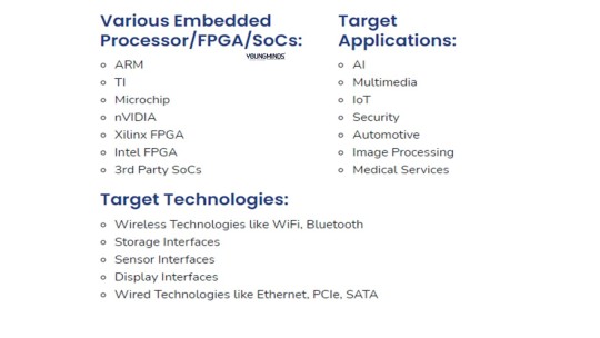
Firmware Development and Optimization of Embedded Designs for a wide range of processors.
Various Embedded Processor/FPGA/SoCs:
ARM
TI
Microchip
nVIDIA
Xilinx FPGA
Intel FPGA
3rd Party SoCs
Target Applications:
AI
Multimedia
IoT
Security
Automotive
Image Processing
Medical Services
Target Technologies:
Wireless Technologies like WiFi, Bluetooth
Storage Interfaces
Sensor Interfaces
Display Interfaces
Wired Technologies like Ethernet, PCIe, SATA
Still need more information about “Young Minds” – Visit https://ymtsindia.com/
Embedded System Design Solutions: - https://ymtsindia.com/embedded-system-design
0 notes
Text
Hall Effect Sensor Market - Forecast 2022-2027
Hall Effect Sensor Market Overview
The Hall Effect Sensor Market size is forecast to reach US$ 2.1 billion by 2027, growing at a CAGR of 8.6% from 2022 to 2027. Hall effect sensors use ‘Hall Effect’ principle to convert magnetically encoded information into electrical signals. The principle of Hall effect sensors depends on the electron mobility. These devices have a range of applications, with Hall effect sensors often used in automotive systems to sense position, distance and speed. They are commonly used in automotive control systems like proximity sensing, speed detection, anti lock braking systems and others, electronics, and measurement devices. The factors such as rise in industrial automation, growing application of hall effect sensor in robotics, increasing use of programmable and fully integrated current sensors and transducers and wide temperature stability in extreme environments in wide range of industry verticals are helping in the growth of this market. However, the factors such as high cost of raw materials for hall effect sensors and technical issues like inconsistent.
Request Sample
Hall Effect Sensor Market Report Coverage
The report: “Hall Effect Sensor Industry Outlook – Forecast (2022-2027)”, by IndustryARC covers an in-depth analysis of the following segments of the Hall Effect Sensor industry.
By Type of Loop :Open-Loop Sensor, Closed-Loop Sensor
By Rotor:Magnetic rotor, Ferrous vane rotor
By Magnetic field:Unipolar, Bipolar, Omnipolar
By Technology:BiCMOS, CMOS
By Material:Gallium Arsenide (GaAs),Indium Arsenide (InAs),Indium Phosphide (InP),Indium Antimonide (InSb),Graphene
By Output: Analog ( Linear ), Digital ( Switching )
By Application:Position sensing, Motion sensing, Wireless Communication, Pressure Sensing, Flow rate Sensing, Vibration sensing, Others
By End user: Industrial Equipments, Power & Energy, Oil, gas and petrochemical, Automotive, Consumer Electronics, Telecommunication, Healthcare, Aerospace & Defense, Manufacturing, Robotics, Others
By Geography: North America (U.S, Canada, Mexico), Europe(U.K, Germany, France, Italy, Spain,Others), APAC (China, Japan, South Korea, India, Australia, Others), South America (Brazil, Argentina, Others), RoW (Middle East, Africa)
Key Takeaways
The open loop sensor segment is predicted to grow at a faster rate than closed loop sensor overthe forecast period of 2002-2027 in the Hall Effect Sensor Market segmented by type of loop. This is owing to more precise results with simple design, cost effective circuit and easy to maintain and tune.
The industrial segment held the largest share in Hall Effect Sensor Market by application, in 2021. This is attributed toadvent of industrial automation and need of accurate production lines for safety and efficiency.
Asia-Pacific (APAC) market held the largest market share of 35%, in 2021. This is due to growing research in Hall Effect sensor technologies, rise in industrial automation and robotics and government policies to boost the semiconductor sensor industry.
The increasing smart grids and robotics in industries, growing use of electric vehicles and smart automotive systems and growing research in Hall Effect sensors for improved performance are the contributing factors in the growth of Hall Effect Sensor Market.
Inquiry Before Buying
Hall Effect Sensor Market Segment Analysis - By Type of Loop
The Hall Effect Sensor Market by type of loop has been segmented into open loop sensor and closed loop sensor. The open loop segment is predicted to grow at a faster rate with CAGR of 9.8%, over the forecast period 2022-2027. This is owing to growing application of open loop hall effect sensors in industrial equipments, ease of implementation of the mechanism and galvanic isolation effect. Open loop current sensors consist of a Hall sensor mounted in the air gap of a magnetic core. An open-loop Hall-effect sensor uses the Hall voltage directly to produce its output signal making it simpler to implement and exhibits a faster response time. These sensors help improve the overall efficiency and productivity of an automation process due to galvanic isolation effect. It is a major factor in the selection of a open loop hall effect sensor mainly for current measurement applications. Thus, open loop hall sensors have several benefits in industrial applications which are mainly promoting the growth of this open loop hall sensor segment. In July 2021, a customized version of LEM’s HAH1, an open loop hall effect sensor, was developed. It significantly reduces the assembly footprint compared to previously available solutions and allows a higher integration level within the control infrastructure. Thus, growing use of open loop Hall Effect sensor with integrated systems and customized structure as per requirement is fuelling the growth of this market
Hall Effect Sensor Market Segment Analysis - By End User
The Hall Effect Sensor Market by end user has been segmented into industrial equipments, automotive, consumer electronics, telecommunication, healthcare, aerospace & defense, manufacturing, others. The industrial equipment segment held the largest share of 32%, in 2021. This is owing to the increasing need of precision production line processes and wide working temperature range in extreme industrial environments. Current sensor, pressure sensors and rate of flow sensors are some of the extensively used applications of Hall Effect sensors in industrial and manufacturing. In Industrial equipments, Hall Effect sensors are used in security systems, alignment controls, micrometers, machine tools, key switches, linear potentiometers, rotary encoders, and brushless DC motor commutators. Thus, a large scale of equipment and process line requirement of Hall Effect sensor in industrial applications is assisting the industrial equipments segment growth. In October 2021, Texas Instruments has introduced TMAG5170, the first device in a new family of 3D Hall-effect position sensors for real-time control in factory automation and motor-drive applications. The sensor is promoted as providing integrated functions and diagnostics to maximize design flexibility and system safety while saving energy. Such growing advancements in hall effect sensor technologies for industrial requirements and other applications is driving the growth of this market
Schedule a Call
Hall Effect Sensor Market Segment Analysis - By Geography
The Hall Effect Sensor Market by geography is segmented into North America, Europe, Asia-Pacific (APAC), South America, and the rest of the world (RoW). Asia Pacific (APAC) held the largest Hall Effect Sensor Market share with 35% of total market size. This is due to increasing government policies supporting industrial automation and growing research in new technological integration in Hall effect sensors such as 3D sensing or bipolar complementary metal-oxide-semiconductor (BiCMOS) technology in countries such as China, India, South Korea, and Japan. The recent developments of graphene-based Hall Effect sensors, programmable hall effect sensors are also boosting the growth in Asian countries. In June 2020, Melexsis announced an automotive grade monolithic sensor that uses Hall Effect to provide contactless sensing in three-dimensional environment. The dual die version of MLX90395 is defined through system processor, rather than hardwires into device. Such, growing innovations in the Hall Effect sensors is accelerating the growth of this market in Asian countries.
Hall Effect Sensor Market Drivers
The rising industrial automation and increasing use of smart grids in production line boosts the growth of Hall Effect Sensor market
The Hall Effect Sensor Market is growing due to the rise in demand for sensors with higher accuracy levels, wide working temperature ranges and accurate results. The increasing use of smart grids and rising safety concerns within industrial applications drive the demand of hall effect sensors. The rise in implementation of industry 4.0 technologies such as industrial internet of things (IIoT) and cloud-computing has created high demand for variety of sensors. Another essential part, DC motors, and switches, controls also use Hall Effect sensors for automation which are increasingly used by various industries. Hall effect sensors are also an effective, contactless way to measure DC magnetic flux in current transformers. These sensors dedicated for different kinds of industrial applications are available for example, sealed Hall Effect devices are water-proof and are made in such a way to resist any vibration. Thus, customization of these sensors is assisting in the growth of this market. In January 2022, Allegro MicroSystems, Inc., a global leader in sensing and power solutions for motion control and energy-efficient systems, announced its new A33230 3D sine/cosine Hall-effect position sensor IC. The A33230 is the smallest 3D sine/cosine sensor currently available in the market, and offers system designers a cost-effective solution for automotive and industrial applications with a quick time to market. Thus, growing industrial applications is driving the Hall Effect Sensor Market growth.
Buy Now
The increasing research in bipolar complementary metal-oxide-semiconductor (BiCMOS) technology, intelligent hall effect sensors and three-dimensional sensors is boosting the hall effect sensors market growth.
There are growing advancements in the Hall Effect sensor technologies such as BiCMOS, three-dimensional and many others. BiCMOS offers a high current drive per unit, low input density, high power dissipation, and low noise compared to conventional or CMOS technology. A BiCMOS chopper stabilization circuit is utilized to reduce signal offset and to stabilize the output of the IC over its operating temperature range. with BiCMOS technology, features fast power-on time and low-noise operation. A family of Hall-effect sensors optimized for automotive and mechatronic applications that demand accuracy and flexibility combined with low cost. It includes a microcontroller, a temperature sensor, advanced on-chip compensation, and a digital interface. The latest automotive designs require smart sensors to deliver the high level of precision and robustness linked with the capability of local pre-processing of the measured data. In May 2022, Synaptics Inc. has launched the FlexSense family of sensor processors that captures and intelligently handles input from up to four sensors in a tiny, ultra-low-power form factor that is up to 80% smaller than existing solutions. Integrating a mix of capacitive, inductive, Hall effect and ambient sensing into a single processor with proprietary algorithms, the FlexSense family brings reliable, low-latency, and context-aware force, proximity, and touch sensing to Internet of things (IoT) devices. Such innovations in integration of hall effect sensors with intelligent technologies is driving the growth of this market.
Hall Effect Sensor Market Challenges
The issue of uneven strength of magnetic fields in Hall Effect sensors is restricting the growth of this market
Hall effect sensors produce an output voltage directly proportional to the strength of the magnetic field generated by the current supplied. It is connected to an analog to digital (A/D) converter, microprocessor, or microcontroller to maintain the voltage. Hall-Effect sensors work on the concept of magnetic field, which makes them more vulnerable to external magnetic fields, leading to inconsistent measurement of the current flow. These sensors are not suitable for measuring the flow of current if the distance between the generated magnetic field and the current-carrying conductor is beyond certain limits which is expected to hinder the market growth. In May 2022, Titan Enterprises Ltd, explains some of the reasons for sensor failures. High quality Hall effect sensors are typically used within Titan’s pulse precision flow measurement devices. The sensors operate between 4.0Vdc and 30Vdc, however, exceeding the maximum 30Vdc to the Hall Effect sensor will damage the unit. A good quality regulated DC power supply is recommended for powering a pulse flow meter. Thus, due to the technical limitations and need to maintain certain distance and current flow restricts the growth of this market.
Hall Effect Sensor Market Landscape
Product launches, acquisitions, and R&D activities are key strategies adopted by players in the Hall Effect Sensor industry. The Hall Effect Sensor top 10 companies include:
ABB Ltd
Allegro MicroSystems LLC
TE Connectivity Ltd
Bartington Instruments Ltd
Honeywell International Inc.
Analog Devices, Inc.
Robert Bosch GmbH
NXP Semiconductors N.V.
TDK Corporation
Infineon Technologies AG
Recent Developments:
In July 2020, Texas Instruments announced the industry’s first zero-drift Hall-effect current sensors. The TMCS1100 and TMCS1101 enable the lowest drift and highest accuracy over time and temperature while providing reliable 3-kVrms isolation, which is especially important for AC or DC high-voltage systems such as industrial motor drives, solar inverters, energy-storage equipment and power. This product with unique feature and varied applications will aquire a significant market share
In May 2021, Paragraf continues to push performance boundaries with its graphene Hall Effect sensors. Oxford Instruments, a leading provider of high technology tools and systems for research and industry, have employed a modified version of the Paragraf GHS09CC sensor device to carry out measurements at temperatures and magnetic field strengths far beyond the scope of any other sensing solution. Thus, this breakthrough innovation of using graphene will help in gaining a significant market share.
In October 2021, Texas Instruments has introduced TMAG5170, the first device in a new family of 3D Hall-effect position sensors for real-time control in factory automation and motor-drive applications. The sensor is promoted as providing integrated functions and diagnostics to maximize design flexibility and system safety while saving energy. Thus, expanding the integration and advanced features will assist in capturing the market of hall effect sensors.
In November 2021, TDK Corporation announced the portfolio expansion of its Micronas direct-angle Hall-effect sensor family with the HAR 3927. This product uses proprietary 3D HAL® pixel-cell technology and addresses the need for ISO 26262-compliant development. Various configuration options of HAR 3927 increase customers’ flexibility during development and enable one sensor to be used in multiple applications, which reduces costs and effort for re-qualification. Thus, compliance with certification and improved results will help in market growth of hall effect sensors.
0 notes
Text
Knowing More About Printed Electronics
Printed electronics is the integration of organic semiconductor electronics in print products. It is one of the primary applications in the field of functional printing and is a complement to conventional electronics.
The following features distinguish printed electronics:
It is based on flexible substrates made of specifically functionalized polymer films (plastic semiconductors).
It can be designed over a large area.
It is less than a millimeter thick.
In which processes are printed electronics produced?
Printed electronics - to be more precise: the semiconductors made of plastic - can be produced efficiently and increasingly cost-effectively in mass printing.
Three methods are essentially used for this:
Screen printing
Flexographic printing
Inkjet printing
Electronics printed using the screen-printing process
Screen printing can produce thick layers of impasto materials and is therefore used for printed electronics' industrial production. This process has, for example:
Conductor tracks made of inorganic materials, e.g., B. for circuit boards, antennas, or glucose test strips
insulating passivation layers
Electronics printed using flexographic printing
The flexographic printing process offers several properties that benefit the production of printed electronics:
The flexible printing forms are produced using direct laser engraving, which enables very fine structures.
The cleaning of the printing forms after lasering is done with water. This means that no solvents are needed.
Inks and pastes with conductive, magnetic, hydrophobic, photoconductive, or corrosive properties can be printed.
For example, printed circuit boards, sensors, or memory labels are produced in flexographic printing. But the process can also be used for RFID antennas or smart packaging, for example, for pharmaceuticals.
Electronics printed using the laser inkjet process
Examples of printed electronics using the laser inkjet process are applications from the circuit board and ceramic industries. The special thing about the process - the so-called lasersonic process - is that the drop is emitted directly from a color film's surface instead of from a nozzle by laser bombardment and is thus transferred directly and without contact to the printing material. Besides commercially available printing inks, lasersonic can also print many functional pigments.
With the laser inkjet process, the entire color space that conventional printing presses also use can be used digitally for the first time. Expensive printhead changes should be a thing of the past with lasersonic technology, as should expensive special inks.
What are applications Printed electronics needed for?
There are now several applications where printed, and organic electronics are needed and are even on their way into broad mass markets. Integrated systems printed off the roll are inexpensive, compact, and energy-efficient. Conductive polymers are already being produced in large quantities using printing technology.
Examples of electronic applications are:
Consumer goods
Industrial controls
printed antennas and sensors for the automotive industry
Antistatic coatings
OLED displays (organic light-emitting diode displays), e.g., B. for navigation devices or air conditioning systems
Electroluminescent displays
organic photovoltaics (OPV), i.e., the production of solar cell elements
electronic product label to protect against counterfeiting
Temperature sensors for food packaging
The transition from micro to nanotechnology will probably open up entirely new perspectives for print applications.
1 note
·
View note
Text
Buy Word Class Equipment and Tools for Electronics in Delhi
Ionised air gun neutralise static fees on several materials as well as clean the surface area using ionised compressed air. Neutralising the static charges makes it easier to blow-clean the surface and avoids dust as well as dirt fragments from being re-attracted.
Static eliminators or static ionizers remove static as well as dust as well as can counteract and clean surface areas at remote ranges. Static neutralization is a functional technique of static reduction; nevertheless complete static elimination is not readily possible.

Electrostatic field meter is utilized to situate as well as measure static charges. It is extremely small, pocket dimension and also basic to use. It has the adhering to functions which are operated by pushbuttons: Power on/off, absolutely no adjustment, Ion Equilibrium and also Hold. Utilize the hold switch to retain the display screen of the analysis.
Ion bars are developed to regulate static charge in mini-environments, laminar flow hoods and also workstations. Ionizing bars include distinct aerodynamic layout that ionizes an area without interrupting laminar circulation. Installation is quickly.
We provide Static Charge Removal system with Static System Guard. Made using luxury technology, this system is made use of to remove all opportunities of dangerous results on personnel as well as product, therefore help in providing high effectiveness in terms of manufacturing, top quality, less male hour and higher revenues. Our system is utilized by customers in various markets, ranging from Textiles.
A digital multimeter or DMM is one of the most widely utilized pieces of test devices today. DMMs are available extremely inexpensively as well as these digital multimeter can provide extremely high levels of precision when measuring the specifications within an electronics or electrical circuit. Because of this, DMMs are just one of the most vital items of test devices offered today.
A Digital clamp meter is an electric examination device that integrates a standard digital multimeter with a current sensor. Probes gauge voltage. Having a hinged jaw incorporated right into an electrical meter allows service technicians to secure the jaws around a cord.
A digital tachometer is a digital device that determines and shows the speed of a turning object. A turning object might be a bike tyre, an auto tire or a ceiling fan, or any kind of various other motor, and so on. A digital tachometer circuit comprises LCD or LED reviewed out and also a memory for storage space.
Lux meters are made use of for gauging brightness in lux, fc or cd/m ². Some lux meters are outfitted with an interior memory or data logger to document as well as conserve measurements. The dimension of light intensity with a Lux Meter is Lux meter Review ending up being increasingly essential in the office because of security worries.
Portable insulation resistance testers and also megohmmeters are designed to aid avoid hazards such as electrical shock as well as short-circuits triggered when the insulation in electric gadgets, components, and also devices made use of in plants, structures, as well as various other setups deteriorates over extended periods of use.
A soldering iron is a hand tool made use of in soldering. It provides warm to melt solder so that it can stream right into the joint between 2 job pieces. A soldering iron is made up of a warmed metal idea and also a protected handle. Home heating is usually achieved electrically, by passing an electric current (provided via an electric cable or booster cable) via a repellent heating element.
Flux Cleaner is created to remove the burnt or clear deposit that flux leaves after the heat-treating procedure is complete. When is made use of as a change for soldering electrical calls especially those that accuracy parts snugly surround taking advantage of an aerosol change eliminator gives a number of advantages over making use of a Flux cleaner in tidy kind.
A soldering station Appears complicated-- and expensive. But it's not. It's simply a soldering iron with a built-in thermostat and a huge external power supply to maintain it at a constant, hot-but-not-too-hot temperature level as it melts solder as needed. And now they're available for under $50.
The Digital Soldering as well as Desoldering Station is a high performance and multi-function station for electronic product research, manufacturing as well as rework. We generate the very best soldering as well as desoldering options including digital soldering station in India.
In any SMD Rework Station or warm air blower, there are two control handles. One control knob is to regulate circulation of Hot Air while the various other control handle is made use of to control temperature level. Hot air flows through nozzle attached to the take care of.
Soldering without any No Clean Flux is a useful option for getting rid of the tedious message solder cleaning utilizing pricey as well as also contaminating CFC solvent cleaning. No Clean Change are reduced strong (much less than 5%) changes, especially produced for SMDs and also blended technology soldering.
VOC-free Flux use water as the leading solvent. Along with restricting the quantity of volatile organic compounds (VOC) right into the atmosphere, sometimes associated with international warming, VOC-free Flux is also non-flammable.
An Electric screwdriver is a tool, guidebook or powered, for screwing as well as helping to loosen (positioning as well as additionally eliminating) screws. A regular simple Electric screwdriver has a take care of along with a shaft, ending in a suggestion the individual takes right into the screw head prior to changing the handle.
Pneumatic Screwdriver use compressed air and also ideal for low-torque applications such as woodworking or sheet steel repairing.
Digital screwdrivers made for accuracy application as well as measurement of torque in manufacturing as well as lab settings. Digital as well as dial torque screwdrivers in supply for a wide variety of applications.
Torque meter is readily available in two different versions: portable meters or table leading meters. Torque meter have a wide variety of applications. Portable torque meter is generally made use of for industry while table leading torque meter is the suitable tool Torque meter summary for research laboratories.
Epoxy Dispenser Option
The Epoxy Dispenser is a regulated system. The epoxy dispenser has a Rotating Layout Positive Variation Pump with a brand-new better resolution electric motor. This indicates has even far better performance.
Use of Desoldering Wick
Use of Disordering Wick variety from actually minute straight-forward jobs to tough applications based upon the need as well as additionally application, numerous Wick are conveniently available, varying in power usage, temperature level array, microcontroller (MCU) based control as well as additionally various other features.
Soldering robo automate the Manual soldering process. A soldering iron installed throughout effect of the robotic is relocated to previously configured placements, where it will certainly solder the joint. The required solder in the kind of readily available solder cable is being fed through solder cord feeders to the joint to be made.
How to Use of a Solder Pot
Solder pots are little, temperature-controlled pots or containers with flared lips that are made use of two tin cords as well as soldering tips. Solder pots also are especially useful for dipping electronics such as printed motherboard (PCBs) with through-hole leaded elements. Solder pots are utilized in smaller sized commercial applications or in nations where modern technology isn't as easily accessed.
If you have any questions, please contact us at [email protected] or +91-9599592691. We at Advance Tech Services (P) Ltd, offers Equipment, Tools & Consumables for Electrical, Electronics, Automobile, Pharma Industry and other commercial applications, including Electronic Maintenance at reasonable cost in Delhi.
#soldering robo#desoldering wick#epoxy dispenser#torque meter#Digital screw driver#pneumatic screwdriver#electric screwdriver#voc free flux#no clean flux#SMD Rework station#desoldering station#soldering station#flux cleaner#Soldering Iron#Insulation Resistance Tester#Lux Meter#digital tachometer#Digital clamp meter#digital multimeter#static charge removal systems#ion Bar#electrostatic field meter#static eliminator#ionised air gun
1 note
·
View note
Text
Painting Masking Tapes Market:2027 Report Analysis by Growing Demands, Current and Future Trends
Painting Masking Tapes Market was worth US$ 34.81 Bn in 2020 and total revenue is expected to grow at a rate of 9.56 % CAGR from 2021 to 2027, reaching almost US$ 65.96 Bn in 2027.
Painting Masking Tapes Market Overview:
Image sensors, control circuits, and interfaces such as Ethernet are all integrated into a Painting Masking Tapes. It is used to monitor traffic and applications that require digital signal processing. Painting Masking Tapess allow high-resolution films and photos to be taken. Smartphone manufacturers have begun to place a larger emphasis on the quality of their cameras in order to differentiate their products. At the Qualcomm Tech Summit in Hawaii, Motorola said that its flagship 5G smartphones with enhanced photography capabilities would be available by 2020. (held recently in December 2019).
In September 2019, One Plus announced the One Plus 7T, which features a spherical Painting Masking Tapes on the back with three horizontally aligned cameras. On the rear, a 48-megapixel primary sensor is joined by 16-megapixel and 12-megapixel cameras that can all shoot wide-angle and 960 frames-per-second slow-motion videos.
The MMR report on the Painting Masking Tapes Market provides Size Analysis and forecasts 2020 to 2027. Industry Research Report is detailed, with all the important factors, to help you in business decisions making and develop crucial strategies. Regardless of a manufacturing process or cost structures, this report provides a comprehensive understanding of the progression strategies and ways.
Market Trends:
The report has analyzed many features which are impacting the growth of Painting Masking Tapes market. Thriving factors are positively impacting the demand and restraining factors obstructing the growth of the market are discussed in detail along with their impacts on the global market. Furthermore, the trends which are driving the market and impacting the growth of the market are identified and discussed in detail in the reported study. Other qualitative and quantitative factors such as risks taking with the operations and major challenges faced by the players in the market are included in the report.
Request for free sample:
https://www.maximizemarketresearch.com/request-sample/64270/
Painting Masking Tapes Market Segmentation:
Global Painting Masking Tapes Market by Type
• Acrylic-based • Silicone-based • Rubber-based • Others
Global Painting Masking Tapes Market by Backing Material
• Foam • Foil • Plastics • Glass Fiber • Paper • Foil
Global Painting Masking Tapes Market by Application
• Painting • General Purpose • High Temperature Applications • Spraying • Metal Working
Global Painting Masking Tapes Market by End-user
• Automotive • Building & Construction • Electricals & Electronics • Packaging • Aerospace • Consumer Goods • Furniture & Decorations • Others
Global Painting Masking Tapes Market by Region
• North America • APAC • Europe • MEA& Africa • South America
Key Players:
• 3M Company
• Berry Global, Inc.
• Nitto Denko Corp.
• Saint-Gobain Performance Plastics Corporation
• Scapa Group PLC
• Intertape Polymer Group, Inc.
• Beiersdorf Aktiengesellschaft
• Shurtape Technologies LLC
• Bolex (Shenzhen) Adhesive Products Co. Ltd.
• Advance Tapes International Ltd.
• Lintec Corporation (Japan)
• Avery Dennison Corporation (US)
• Lohmann GmbH
• abro
• sumax Enterprises
Ask your queries regarding the Report:
https://www.maximizemarketresearch.com/market-report/global-painting-masking-tapes-market/64270/
Regional Analysis:
Asia-Pacific(Vietnam, China, Malaysia, Japan, Korea, Thailand, India, Philippines, Indonesia, and Australia)
Europe(Turkey, Russia UK, Italy, Germany, France, etc.)
North America(the United States, Mexico, and Canada.)
South America(Brazil etc.)
The Middle East and Africa(GCC Countries and Egypt.)
COVID-19 Impact Analysis on Painting Masking Tapes Market:
The COVID-19 pandemic has had an impact on the method of life across the globe. Each business, the industry has got to fight the battle on each front—health and economic. The only reply to this spiral is to strategize through this pandemic disruption, and that we believe that firms shall profit an excellent deal from our report into the market. Our report provides probable solutions to the problems caused by the COVID-19 pandemic
About Us:
Maximize Market Research provides syndicate as well as custom made business and market research on 12,000 high growth emerging technologies & opportunities in Chemical, Healthcare, Pharmaceuticals, Electronics & Communications, Internet of Things, Food and Beverages, Aerospace and Defense and other manufacturing sectors.
Contact us:
MAXIMIZE MARKET RESEARCH PVT. LTD.
3rd Floor, Navale IT park Phase 2,
Pune Banglore Highway,
Narhe,Pune, Maharashtra 411041, India.
Email: [email protected]
Phone No.: +91 20 6630 3320
0 notes
Text
ADS6445IRGCR Analog to digital converter
Analogue-to-Digital Converters (ADCs) allow microprocessor-controlled circuits, Arduinos, Raspberry Pi, and other digital logic circuits to communicate with the real world. In the real world, analog signals have continuously changing values from various sources and sensors to measure sound, light, temperature, or movement. Many digital systems interact with their environment by measuring the analog signals from such transducers. There are different types of ADC when it comes to structuring. The ADS6445IRGCR is a pipeline structured ADC. Pipeline converters determine the digital world through under-sampling with sample/gain algorithm topology or larger cycle-latency.

The ADS6445IRGCR is a high-performance 14-bit pipeline dual-channel A-D converters. The ADS6445IRGCR offers a variety of sampling rates, such as 125/105/80/65 Mega samples per second. The ADS6445IRGCR comes in a compact 48-pin QFN package (7mm × 7mm) with high system integration density. This compact packaging of ADS6445IRGCR is only possible because of Serial Low Voltage Differential Signaling (LVDS) data outputs that reduce interface lines. The ADS6445IRGCR includes a 3.5 dB coarse gain option that can be used to improve spurious-free dynamic range (SFDR) performance with little degradation in signal-to-noise ratio (SNR). In addition to the coarse gain, good gain options exist in the ADS6445IRGCR, programmable in 1dB steps up to 6dB. For convenience, The ADS6445IRGCR also includes the traditional 1-wire interface used at lower sampling frequencies.
Compared with different alternatives available in the market, the ADS6445IRGCR has a few distinct advantages and some drawbacks. The ADS6445IRGCR structure falls into the pipeline category of ADC. The ADS6445IRGCR has one of the fastest sampling rates, up to 1 GHz second only to Flash type ADC. There is usually a trade-off between sampling rate and bit resolution. The ADS6445IRGCR offers a bit resolution of up to 16 Bits which is when compared to other ADCs. However, if a specific application requires a fast sampling rate with minimal bit resolution, then pipeline structured ADC the ADS6445IRGCR is the most suitable candidate.
A few distinct features/Advantages that gives The ADS6445IRGCR an edge over its competitors include
· 14-Bit Resolution with No Missing Codes
· Simultaneous Sample and Hold
· Serialized LVDS Outputs with Programmable Internal Termination option
· Internal Reference with External Reference support
· No external decoupling is required for references
Due to these characteristics of the
ADS6445IRGCR
, they are used in various applications that require fast sampling rates. These applications include Medical Imaging (Oscilloscopes), Diversity Receivers, Base station If receivers, and test pieces of equipment
0 notes
Text
Analog and Mixed Signal Device Market Segmentation And Opportunity Analysis Report till 2022
September 14, 2021: Mixed signal devices are those that can process both analog and digital systems in a single system. The system can be in the form of a hybrid microcircuit, single integrated circuit chip or a printed circuit board. DACs and ADCs are applications of mixed signal processors as both digital and analog functions are implemented in each. Very large scale Integration(VLSI) is another application that employs processing complex digital signals and analog processing on the chip simultaneously.
Improving technology trends and current markets have increased the demand for mixed signal integration. They have significant benefits and can result in innovative System on chip (SoC) solutions. Integrating analog with digital modules have efficient functionality and power consumption owing to better distribution Single chip solutions. Mixed Signal devices have reduced system noise and faster switching times. They also have simple system designs. Analog modules within these devices can be easily controlled by installing inbuilt software.
Creating special functions by leveraging analog modules and integrating it with mixed signals can push performance to new levels and can spur many innovations. These modules available in the market can be integrated into systems to produce special system function solutions can provide high degree of analog integration variables along with low power performance that can reduce costs. These enhancements in the system can provide unique solutions that are fully programmable that are accountable for a substantial cost savings.
Request a Free Sample Copy of this Report @ https://www.millioninsights.com/industry-reports/analog-mixed-signal-device-market/request-sample
Crossover filters in loudspeakers, stereos and controls on TV are other applications of analog processing. Capacitors, resistors, inductors and transistors are common analog processing elements. Analog signal devices can be used in a various market that include aerospace, communication, healthcare, automotive, motor power control, instrumentation and measurement, security and surveillance, Consumer market and Energy sector. Analog processors are significantly cheaper than other technologies available. One challenge with analog system that are exposed to high temperatures is managing their complexity while maintaining the stability of the system.
They play a crucial role in the semiconductor industry where analog to digital conversions are extensively used for the purpose of micro-controllers and signal processing.
One of the important examples of Mixed Signal devices is the mixed single Integrated chips that form a necessary part of the FM tuning in digital devices such as music players that have amplifiers. Introduction of 3G cell phones along with other technologies that are handy, with their increasing usage have a scope of significant growth in the telecommunications market. Availability of ADC and DAC provide a flexible platform for mixed Signal devices as per requirements and are energy efficient.
Considering the advancements in the Mixed signal device market, the task of combining analog and digital signals to optimize performance and integrate them into a single technology has been simplified. New technologies like CMOS, BiCMOS, CMOS SOI and SiGe have nullified many complexities that were faced previously. Availability of different alternatives to cancel out noise disturbances such as fully differential amplifiers, P+ guard rings and on chip coupling have also simplified tasks.
Every industry has specific requirements and configurations. The consumer electronics include touchscreen devices, display drivers, LED drivers, audio and video codes. The Industrial sectors includes devices like energy monitoring, LED Lighting, ADC, RF and line drivers. The automobile industry includes ADC and sensors. In the computer and storage devices market, Analog and mixed signal devices can be found in SATA, HDMI and Thunderbolt. Communications sector constitutes clock and timing control.
Power management sector, Signal processing sector are segments than can be expected to have high growth. The power sector accounted for over 52% of Analog Integrated Circuit Consumption. This sector emphasizes on efficient utilization of power used by electronic devices. Analog ICs are majorly used in portable devices which are extensively used. Other major functionality includes reduction in the battery drain that indirectly reduce costs. Hence with the growth in the wireless communication market can lead to growth in the Analog IC market.
Increase in the usage of application specific Analog ICs can bring about a sales growth of these devices. They constitute for 60% of the Analog ICs Market. With the advent of new technologies in Sensor ASICs and Power Management ASICs, there are wide variety of applications in each of them which include consumer electronic devices such as digital cameras, LCD and LED screens, cell phones and other devices that work on battery.
Market pertaining to analog and mixed signal devices have a diversified customer base. New product innovation and launch of sophisticated instruments can provide new avenues for growth in this industry. Health care industry has wide application of analog and mixed signal devices. They are used as monitoring equipment, medical instrumentation and diagnosis. Firms can differentiate their products by collaborating and integrating different functionalities of design tools and application support systems. Increasing usage of smart phone devices is also a major market for analog and mixed signal devices they are used as chips within smartphones.
Browse Full Research Report @ https://www.millioninsights.com/industry-reports/analog-mixed-signal-device-market
New product Developments are expected to play a major role with the introduction of EDA tools that are specifically made for analog/mixed signal market. The Market is expected to grow at a rate of 5%. Costs associated with processes are usually balanced out with the new avenues in the various product developments in the market.
With the focus of these technologies seen in Europe, Asia, Japan and U.S., the market is majorly driven by best.tools and methodologies that can be employed in the field of aviation, automobiles, communications, multimedia sectors and telecommunications. Opportunities include new modelling techniques, Analog Modeling and RF Modeling. Modularizing capabilities and enhanced integration with different systems of advanced packaging and SoCs.
Competitors in this market include Analog devices that is a market leader in National Semiconductors, Maxim Integrated Products Inc., and Texas Instruments, BroadComm QualComm, Linear and Maxim. Most competitors are characterized by high operating margins and gross margins. Analog and Mixed device manufacturing firms are highly resource intensive employing many applications that are involved in development, sales, sales reps, and distributors.
Get in touch
At Million Insights, we work with the aim to reach the highest levels of customer satisfaction. Our representatives strive to understand diverse client requirements and cater to the same with the most innovative and functional solutions.
Contact Person:
Ryan Manuel
Research Support Specialist, USA
Email: [email protected]
0 notes
Text
Advances in Real-Time Soil Fertility Determination- Juniper Publishers

Rapid advances in sensor technology are enabling aggressive use of informatics in agriculture. This paper focuses on applying the newly developed soil electrical impedance spectrum sensor combined with artificial intelligence to predict soil fertility. The described method determines the type and amount of fertilizer to be used. The proposed sensor system is portable and fast enough for real-time measurements in the field using a slow-moving tractor. It is affordable, battery-powered and allows wireless data transmission to the farmer’s soil database. Such a database allows the farmer to create a reliable fertilizer plan. The crop is of better quality because fertilizer is applied only where it is needed on the plot. The use of fertilizer is optimized, costs are reduced, and the environment is preserved. Many papers report more or less credible results on this problem, but they lack verification of real conditions in the field.
Keywords: Soil analysis; Real-time fertilization plan; Electrical impedance spectrum of the soil; Soil classificatory
Abbreviations: Application Specific Integrated Circuit (ASIC); Deionized (DI); Agriculture Institute of Slovenia (KIS); Principle of Component Analysis (PCA)
Introduction
The diversity of soil conditions in terms of its moisture, composition, texture, and temperature makes soil analysis very difficult. The deterministic methods, such as chemical analysis, cannot be used in the field because it requires a chemical laboratory. It is time consuming, expensive and unreliable as it only relates to a particular soil sample. Dozens of soil samples must be collected and analyzed per acre. In the recent article [1], the authors described their vision about the future development of digital agriculture. They listed several possible sensors that would monitor the agricultural plot and collect a soil and crop status database below and above the surface. The analysis of this data would pave the way for the optimization of agricultural activities. Many methods have been described [2-4], but none are accurate enough or acceptable for real-time applications. We want to collect soil fertility results in a few seconds while driving the tractor over the field. In this section, we will briefly review some of the most promising soil characterization technologies. Optical methods were investigated using spectral analysis in both the visible and visible-infrared spectra, analyzing either reflectance or transmittance results. Our investigation of these methods did not meet our expectations. We tried an interesting approach to study the residual of tiny dried droplets of soil extraction fluid and found promising results. This approach is shown in Figure 1. Figure 2 shows the optical spectra of such a soil solution. Some other impressive results can be obtained under laboratory conditions, but field application is not feasible. Raman spectroscopy or mass spectroscopy analysis is too expensive and too slow for on the fly analysis. The non-contact methods using microwaves and terahertz waves are too expensive and not convincingly reliable. Unfortunately, these methods have not met the expected criteria. We need a better approach that is marketable and accepted by farmers. In our study, we decided to develop a sensor system that meets the following criteria for acceptance:
a.accuracy, reliability, and repeatability,
b.fast, on the spot, portable, battery-powered,
c.easy to use, robust and user-friendly,
d.low cost, and
e.ready for wireless communication.
The closest technology to meet the listed requirements seemed to measure and analyze the soil’s electrical impedance spectrum. The soil electrical impedance spectrum method [4] is the most promising, but it requires significant extensions to meet the listed acceptance criteria. In the following sections we will describe these extensions.
Materials and methods
In the field, the soil sample has unknown composition, texture, and moisture. These values significantly affect the soil spectrum and affect soil classification and fertilizer prediction accuracy. In laboratory experiments, these conditions are known and held constant. However, to classify an unknown soil sample, some additional soil parameters must be recorded. These are the relative soil viscosity, the temperature, the value PH and the DC resistivity. These values are used to pre-select a reference database for the classification algorithm. The resulting classification algorithm is then significantly improved. These improvements mean that the soil database of known chemical parameters must be expanded to include the listed parameters. Figure 3 shows the flow-chart of the classification algorithm procedure. Figure 4 shows a simplified schematic of the soil impedance spectrometer Application Specific Integrated Circuit (ASIC). It consists of a mixed-signal design of the front-end electronics, a programmable clock generator to excite the soil sample, and the signal processing unit to calculate the impedance’s real and imaginary parts. Figure 5 shows the simplified interface diagram between the ASIC of the soil impedance spectrometer and the processing unit, like a personal computer or similar. Soil samples are collected from 0-30 cm soil surface and then prepared in the laboratory for characterization and classification. The soil samples were air-dried and sieved 2 mm. They were then mixed with the required amount of Deionized (DI) water to obtain a soil mass with the required viscosity. The amount of DI water is different for each soil and is estimated automatically. A certified laboratory performed a chemical analysis of all soil samples in the Agriculture Institute of Slovenia (KIS) [4]. The comprehensive characterization of each soil sample contains information on all common soil constituents, and only the analyzed nutrients are listed in Table I. Reading and storing the imaginary and real parts of signals corresponding to a soil sample or reference circle is performed using Matlab software. The Matlab script is created to read the controller Analog to Digital Converter (ADC) data and store it in a personal computer or database for further processing.
Data preprocessing is performed to calibrate the obtained imaginary and real parts of soil impedance with the imaginary and real parts of the reference circuit impedance. This procedure is necessary to ensure accurate data acquisition. The reference circuit signals for the final sensor design are measured only once and used to correct other signals acquired with this sensor. We use the corrected signals corresponding to the soil samples to calculate the impedance magnitude and impedance phase. A training set for machine learning is formed from the research dataset measurements corresponding to soil with known chemical properties of phosphorus, potassium and magnesium. The research dataset consists of impedance strengths and impedance phases corresponding to a soil sample. The chemical analysis of soil sample properties performed at KIS includes nutrient values for phosphorus, potassium and magnesium. Tables 2&3 and Figure 6 show the principles of soil sample code formation. Following the fertilizer planning recommendations, the A-E classification was used for each soil component (e.g., phosphorus, potassium, and magnesium). These classification components are then combined to form a XXX code for classifying and predicting the soil properties under test.
The training process includes the feature selection procedure [5] and classification using the so-called “classifier”. Many classifiers have been proposed in the literature that performs classification with different degrees of accuracy. A comparative analysis was performed to select the classifier with the best results (i.e., the best match between the predicted nutrient content and the actual nutrient content determined at the KIS). The classification accuracy was validated using the leave-one-out method [6]. Only soil samples with known chemical properties were used in this validation (i.e., training set). Three subsamples represent each soil sample to allow more accurate analysis. First, a soil subsample corresponding to the measurement from the research dataset was used as a test sample, while the others were used for machine learning (i.e., training set). Then, the obtained prediction is compared with the actual soil properties (i.e., KIS code). This procedure is performed for all data from the research dataset. The results obtained for three subsamples of the same soil are averaged and used to calculate the overall classification accuracy. In other words, the percentage of predicted characteristics that match the certified laboratory characteristics is used to characterize classification accuracy. Taking three or more measurements of the same soil sample is typical in agricultural informatics to obtain a more accurate and representative result. The procedure for calculating the classification accuracy is shown in Figure 7, where the process is illustrated graphically. During the feature extraction procedure, the signal frequencies with the most relevant information for classification are selected separately for impedance magnitudes and impedance phases. Several feature selection methods are described in the literature. The Principle of Component Analysis (PCA) is selected here as one of the most common and useful [7]. An example of the classification accuracy obtained when the feature selection procedure was used and when the feature selection was not used can be seen in Table IV. It shows a significant performance improvement of the classifiers with feature selection even in the problematic soil sample without using the pre-selection feature introduced in the proposed novel classifier. Figure 8 shows the estimated weights for impedance variables according to the research dataset. The threshold value Th=0.2 is used to reduce features with a small impact on classification accuracy. Thus, 13 features were extracted. Table V shows the frequencies and their indexes obtained during feature selection. The obtained frequencies are then used for both machine learning and test signal properties prediction. Tree Bagger [8] was selected as the most promising classifier. Tree Bagger chooses a random subset of predictors for each decision partition as in the random forest algorithm. The outputs of the classifier are model parameters that are unique to each research dataset. These parameters are estimated once and then used to predict the chemical properties of the soil under study. Table VI shows the classifiers selected for comparative analysis in this research.
Results
Table 4 shows the results of the prediction accuracy of the soil sample codes for the research dataset consisting of 21 soil samples collected from different locations in Slovenia with different textures and chemical properties. The feature selection procedure for this dataset estimated five frequencies with weighting parameters greater than Th=0.2. We can see different classification accuracies between the results, with Tree Bagger and Fitcecoc showing the best performance. The least accurate result was obtained using the k- Nearest Neighbor method (i.e., Fitknn). These results are quite acceptable as they have an accuracy of almost 90%. Knowing that the soil sample does not have representative nutrient contents, we can rely on the reasonable assumption that the fertilization schedule is calculated at many points in the studied field since the soil classification is extremely fast. Consequently, the field is mapped in terms of nutrients with a grid sufficient to determine a reliable average fertilizer rate and the proper mix to improve fertility near optimum.
Discussion
The goal of the presented study was to develop an optimized classification algorithm and a portable classifier that can predict the content of nutrients in the soil in a short time. Mapping the soil’s nutrient content on a particular plot is no longer an expensive and time-consuming affair with this device. The fertilization schedule can be automated with a Global Positioning System (GPS) controlled metering device on the farm tractor. The described soil prediction was tested on five different farms on three plots. The analysis was carried out twice a year under different weather conditions and soil moisture. The test sites were selected to represent the diversity of the Slovenian landscape. The first selected farm was located in the NW (North-West) of Slovenia. The soil there is not very fertile, but it was managed for growing seasonal vegetables with a well thought out crop rotation. The second farm is located in SE (South-East) of Slovenia. The soil there is poor and neglected, very muddy and difficult to analyze. The location of the third farm is on the eastern border of Slovenia. The crop there is grown in large plastic tents with automatic irrigation and ventilation. The fourth farm is located in the eastern part of Slovenia. The analysis was carried out on three different vineyards. The soils were clay type and challenging to analyze. The additional feature of the algorithm helped to overcome this and provided the correct prediction. A very similar problem was found in a vineyard in the central-eastern part of Slovenia. Again, the new prediction algorithm proved to be correct.
Conclusion
This paper describes an improved method for determining the electrical impedance spectrum of soil that provides a reliable, robust, and cost-effective tool for characterizing the soil fertility of an agricultural field and for developing an optimal fertilization plan. This project’s result is a portable device for analyzing the soil’s electrical impedance spectrum and characterizing it based on the spectrum data. The system is battery powered. It also allows for direct wireless data transmission. The results were verified in several farms with different soil types. An acceptable probability of correct soil class prediction was achieved. Since the prediction algorithm is based on the principle of self-learning, the probability of correct prediction increases with the growth of the learning data set. We believe that the sophisticated methods described in [9] are not required to achieve such results.
To know more about
Journal of Agriculture Research-https://juniperpublishers.com/artoaj/index.php
To know more about open access journal publishers click on Juniper publishers
0 notes
Text
Why Can’t iPhone Camera See Infrared?
Using Apple iPhone Front Facing Cameras
The front camera of iPhone camera which is facing you allows you to see Infrared. The back camera of the iPhone has an IR filter which filters infrared.
Open the camera app and point to any TV remote and you will see white light when depressing any button of a TV remote of any other kind of remote with an IR light on top of the remote.
Below are the list of iPhones models that can see Infrared
iPhone 4 = front camera can see Infrared
iPhone 7 = front camera can see Infrared
iPhone XS = front and back camera can see Infrared
iPad Pro (9.7″) = front and back camera can see Infrared
iPhone 6 = front and back camera can see Infrared
iPod Touch 5 = front camera can see Infrared
iPhone X = front and back camera can see Infrared
In the world of digital photography, using iPhone front facing cameras is one of the best options for those that want to take the most out of their photography experience.
One of the best features of this device is that it will allow you to see everything that is going on with your subject without having to turn away from the view in order to do so.
This makes the camera perfect for those that like taking pictures while moving around or trying to catch a moving object in the lens.
Some of the best features of this particular camera include the fact that there is no need to worry about getting obstructions in order to get a good shot and that the camera will not only allow you to see the subject but will also allow you to focus directly on it.

In order to take full advantage of your iPhone’s amazing capabilities when it comes to photo taking it is very important that you know exactly how to use the iPhone’s front facing camera.
The first thing that you need to know is that when you are not directly looking at your subject you should move your head to one side slightly in order to gain some eye contact.
In order to accomplish this, you simply need to raise your iPhone up so that you are holding it in the air just above your eyes.
Once you have done this you should focus on looking directly at the camera in order to maximize the amount of light that is coming through the camera.
youtube
How to See How it Works With an iPhone 4
You might be asking yourself “How is FaceTime working with an iPhone, and doesn’t the camera have to have an infrared filter so that I can see through the camera?”
This is a good question, and the first thing you need to know is that most cameras on the market do NOT have an infrared filter built in.
FaceTime uses an IP camera that communicates with your iPhone’s camera via a digital audio signal.
So basically instead of dealing with all of those wires connecting the camera to the computer and back up to your computer, you’re only dealing with a simple digital audio signal.

There are two benefits to this though.
The first being that FaceTime works great with streaming video from websites such as YouTube.
Because of the video compression algorithms the camera has to work extremely fast, and FaceTime is at that point pretty good.
With YouTube however, because there is such a delay between when the video is shot, and when it appears on screen, it’s tough to make a nice long video with the computer and FaceTime.
How Do Security Cameras Work? Include IR LEDs Hidden to Humans But Light Up Scene With Light
If we need a clear demonstration of how security camera systems work then let’s have a look at infrared security cameras, they are so much more powerful than their counterparts which means they have a much better ability to give us clear images and video.
An Infrared security camera uses extremely sensitive integrated circuits which can capture the heat energy of a human body and convert it directly into visible light.
Most cameras use an LED (Light Emitting Diode) on board but the best cameras usually incorporate IR LEDs.
For years now companies such as Panasonic, Sony and Samsung have been using infrared technology to capture high resolution images and video.
They also use other highly effective methods such as image stabilization, image correction etc.
We know that CCTV cameras are used to monitor suspicious activities so by capturing movement we can then see exactly what the person was up to.
So how exactly do security cameras work and what sort of results can they achieve?
There are various cameras on the market from passive Infrared Night Vision CCTV cameras to hard wired cameras using LIDAR.
The passive infrared security cameras are a great choice as they are not prone to the temperature extremes of a building and are able to work in the dark.
Black and White Camera Filters
It is now possible to see what is happening inside your digital camera’s IR filter.
A little known fact is that when you are taking photos using a black and white camera, the IR filter in your camera IR filter is blocked from the infrared light that is sent to your sensor.
If the camera lens is not an infrared lens then this blocking of the infrared light will not occur and your pictures would be perfect.
Have you ever been taking pictures with your black and white camera and suddenly got distracted by something and had to change the camera?
Have you ever stood there for a minute or two and just forgot about the photo you just took? This is all due to your IR filter in your digital camera.
Can My Digital Camera See Infrared radiation That is Only Beyond Red Light?
The camera can see infrared radiation that is just beyond red light from 700nm to 915nm? The camera and red are in the same room, yet it seems to not be a red light at all? Can you see infrared radiation that is only beyond red light from 700nm to 915nm?
If you look at the spectrum of visible light with your eye, and look closely at the visible light, you will see a few things that are red.
Look closer still and see infrared.
This is the kind of thing that the camera can see infrared radiation that is only beyond visible red light.
Can you see infrared radiation that is only beyond red light from this distant? You betcha, that’s why you have red, blue, and green waves.
You are probably asking, “Why can’t my camera see infrared radiation that is only beyond red light?” Well, the answer lies in the infrared filter on the camera.
The infrared filter doesn’t allow red light through, and only allows green and blue light through.
If you use the camera with a red filter, the camera will ONLY see infrared radiation that is outside of the visible red light range.
If you use a green filter, the camera will ONLY see red light, which will force you to think that the red light is being reflected.
Silicon Based Sensors Are Sensitive To Far Infrared
The invisible ones are mostly sensitive to far-infrared (FIR). But this is not true in all the devices. The visible ones are mostly sensitive to NIR. The silicon-based sensors in virtually all visible cameras are sensitive to near infrared (NI) as well.
These visible devices are often sensitive to the far infrared rays.
The visible light does not produce far infrared rays, and hence the visible parts of these devices are not sensitive to the far infrared rays.
So these visible parts of the cameras do not respond to them either. The silicon-based detectors can also detect the infrared rays produced by the sun. All such sensors are not sensitive to the far infrared rays.
You should buy a camera sensor having the above mentioned features.
The silicon based sensors will be very useful for you and your business in the areas of surveillance, security, and crime monitoring.
You should use them for the detection of crime before it occurs and prevent it from occurring. sensors in any area of your business premises. You can either mount them on a wall or a floor stand or place them on a vehicle stand.
How White Spots Look Like – Discover The Reality of IR Photography?
IR appears as white light to the camera, desaturating whatever colour present. As described by Wikipedia: “The electromagnetic spectrum of an IR wave is similar to the optical spectrum of visible light, but without pass-bands or edge effects”.
In other words, while visible light contains multiple colours, IR only has one, red.
The wavelength of an IR laser is generally long enough to penetrate many objects, but short enough to not heat up any of the matter it comes into contact with.
To produce IR, a laser generates a beam with a high frequency that has greater energy than the wavelength of visible light, and therefore passes through many objects without heating them, while visible light only needs a relatively short wavelength to do significant damage.
Because infrared lasers are so long and powerful, they do not require an extremely large photo area in order to capture a substantial amount of IR, which makes them very ideal for use by military and police units.
While the quality of the IR picture can be improved by using a wider aperture (wide apertures), this also increases the amount of scattering of light which can reduce the depth of field and cause blurry pictures.
This effect can be overcome by using wide angle lenses and by using image stabilization, where the camera is moved into a stable position, usually far from the subject, and then the picture is taken with the camera moving into that position.
If you are intending to use IR photography for surveillance, it is important to note that although the camera will appear as if it is focusing on the subject, this is actually the IR lens reflecting off of objects in the foreground and onto the camera sensor.
It is important to note that white spots are not caused by refractive errors, as those can appear in normal images.
Instead, white spots are caused by absorption, due to either a low or high absorbing lens.
Therefore, it is important to only use a high power optic that is capable of producing good levels of IR at the required shutter speed.
Infrared Digital Cameras
Infrared digital cameras are also referred to as night vision cameras because they use infrared illuminators to capture images at night.
The technology that is incorporated into these cameras is rather ingenious in its own right.
Many people do not know that it is actually possible to see in the dark with the use of an infrared illuminator.
If you were to look up at the stars from space or observe terrestrial objects in the night sky using your naked eye you would not be able to see through the darkness but an IR camera can.
What makes these cameras so unique are the fact that they use a series of LEDs behind the lens to capture the infrared light that comes through the front of the lens.
These illuminators are completely invisible.
There is no reflection from the surface of the earth that is reflected from the illuminators behind the lens.
When you look through one of these cameras and look directly at the back side you will see the backside of the illuminator which is filled with a neon green.
This is the very same green that is used behind the lens in everyday cameras.
The illuminator behind the lens uses the infrared energy emitted by the human eye and converts it to electrical energy, which is then captured by the LED behind the lens.
An IR digital camera is perfect for security and surveillance applications because they are highly effective at recording video footage without a need for extra equipment.
When these cameras are used in conjunction with a video recorder, the time spent recording can be greatly reduced since there is not a need for continuous film.
These cameras are also extremely beneficial for monitoring areas such as schools, airports, banks, and even inside the home where vandalism and theft are common occurrences.
Understanding The Demosaicing Process
The process called Demosaicing allows the camera to figure out the colour of an object with a certain amount of black and white.
If the light is more than one colour then it is shown as black.
It used to be very difficult to see an object when using only black and white, which is why the camera was set up so that the pixels were all different colours.
Now with computers it is easier to see an object because all the pixels are now different hues, but this process still has its drawbacks.
In the past, if you wanted to make more than one colour, you had to make extra passes over the image until all the colours came out perfectly.
The first demosaicing process was a very slow process that took over two weeks to complete.
The second, much faster demosaicing process made it possible to see objects in a matter of seconds.
You could demosaicing by hand very easily, but it was very difficult to get a perfect result. Today, computer-aided demosaicing is a much faster process that can give you extremely accurate results. Most of today’s demosaicing equipment operates at the level of a CCD sensor.
TV Remote Bright Irradiance
When you buy a TV, one of the things you may notice is the TV remote control – this is a special device that lets you change your TV’s buttons and navigate through the menus.
The infrared light beam frequency that TV remote controls use is much more precise than the one used by radio receivers.
When you move your TV remote up or down, for example, the infrared light beam that reaches your TV can detect the difference in the beams between the two and adjust the remote accordingly.
The post Why Can’t iPhone Camera See Infrared? appeared first on Infrared for Health.
source https://infraredforhealth.com/why-cant-iphone-camera-see-infrared/
0 notes
Text
Screen Printing Simulations: The Future of The Printing Industry

Print is alive and will probably still be alive in the next decades, maybe centuries. But print only remains attractive if it changes and is constantly evolving. With this in mind, it is important to always be on the lookout for interesting applications that not only make the printed product more valuable, but also provide it with additional practical benefits. And if you take a closer look, there are a number of promising approaches. In functional printing, they include so-called printed electronics, which are increasingly becoming the focus of the printing industry. One of the promising approaches is screen printing simulations.
What is printed electronics?
Printed electronics is the integration of organic semiconductor electronics in print products. It is one of the primary applications in the field of functional printing and is a complement to conventional electronics. The following features distinguish printed electronics:
· It is based on flexible substrates made of specifically functionalized polymer films (plastic semiconductors).
· It can be designed over a large area.
· It is less than a millimeter thick.
Electronics printed using the screen printing simulations process
Screen printing is able to produce thick layers of impasto materials and is therefore used for the industrial production of printed electronics. This process produces, for example:
· Conductor tracks made of inorganic materials, e.g. B. for circuit boards, antennas or glucose test strips
· Insulating passivation layers
What applications are screen printing simulations needed for?
There are now a number of applications where printed and organic electronics are needed and are even on their way into broad mass markets. Integrated systems printed off the roll are inexpensive, compact and energy efficient. Conductive polymers are already being produced in large quantities using printing technology.
Examples of electronic applications are:
· Consumer goods
· Industrial controls
· Printed sensors and antennas for the automotive industry
· Antistatic coatings
· OLED displays (organic light emitting diode displays), e.g. for navigation devices or air conditioning systems
· Electroluminescent displays
· Organic photovoltaics (OPV), i.e. the production of solar cell elements
· Electronic product label to protect against counterfeiting
· Temperature sensors for food packaging
The transition from micro to nanotechnology will in all probability open up completely new perspectives for print applications and screen printing simulations.
Basic knowledge of printing technology: Data creation, printing, further processing
The topics of papers, paper manufacturers and alternative printing materials are addressed as well as the various printing inks and inks that are used in offset printing, digital printing, gravure printing, flexographic printing or screen printing.
Another important part of screen printing simulations and production is print processing, because it is only through folding, stapling, adhesive binding, punching and the like that a book, calendar, brochure, poster, photo book or more can be created from the printed sheets.
In a print shop, bookbindery or other company in the printing industry, speed is always important, because the products not only have to be of high print quality, but also have to be delivered as quickly as possible.
Printed electronics is an outstanding example of revolutionary printing techniques. In summary, it means electronic components manufactured using “printable” functional fluids. The individual layers required for the components are created using known printing processes, e.g., B. screen, flexographic, gravure and inject printing, and can be both insulating, electrically conductive and semiconducting.
0 notes
Photo

Maxim Https://www.slw-ele.com; Email: [email protected]
Maxim
https://en.wikipedia.org/wiki/Maxim_Integrated
Maxim Integrated is an American, publicly traded company that designs, manufactures, and sells analog and mixed-signal integrated circuits.
Maxim Integrated develops integrated circuits (ics) for the automotive, industrial, communications, consumer, and computing markets. The company is headquartered in San Jose, California, and has design centers, manufacturing facilities, and sales offices throughout the world. In the fiscal year 2018, it had US$2.48 billion in sales, 7150 employees, and 35,000 customers worldwide. Maxim is a Fortune 1000 company and its stock is a component of the NASDAQ-100 stock market index. In December 2018, Maxim was re-added to the S&P 500.
History
Maxim was founded in April 1983. Its nine initial team members had a variety of experience in semiconductors design and sales. The founding team included Jack Gifford, an industry pioneer since the 1960s; Fred Beck, an IC sales and distribution pioneer; Dave Bingham, General Electric’s Scientist of the Year in 1982; Steve Combs, a pioneer in wafer technologies and manufacturing; Lee Evans, also a pioneer in CMOS analog Microchip design and General Electric’s Scientist of the Year in 1982; Dave Fullagar, inventor of the first internally compensated operational Amplifier circuit; Roger Fuller, yet another pioneer in CMOS microchip design; Rich Hood, development director for some of the first microprocessor-controlled semiconductor test systems; and Dick Wilenken, who is acknowledged as the father of key analog switch and multiplexer technologies. Based on a two-page business plan, they obtained US$9 million in venture capital to establish the company. In the first year, the company developed 24 second-source products. After that, Maxim designed proprietary products that offered greater differentiation and higher profits.
Logo prior to September 2012
In 1985, the industry was introduced to the MAX600, the first proprietary product to win an industry award and start decades of technical innovation. Maxim recorded its first profitable fiscal year in 1987, with the help of a product called MAX232, and posted a profit every year since it went public in 1988. Annual revenue reached $500 million in fiscal year 1998 and in fiscal 2011 totaled over $2.47 billion. In 2005, Maxim became a Fortune 100 company. Three years later, the company established its Chief Technical Office, and the number of patents rose by 50% over the next two years. In 2010, the company shipped its first analog product on a 300mm wafer.
Technical milestones
Maxim's product portfolio now includes power and battery management ICs, sensors, analog ICs, interface ICs, communications solutions, digital ICs, embedded security, and microcontrollers. In these product segments, the company has made some notable achievements.
On the power front, Maxim introduced nanoPower technology in 2017, encompassing ICs with less than a microamp of quiescent current and ideal for small, portable, battery-powered products. Quiescent current is the largest contributor of a system's standby power consumption. By utilizing components with low quiescent current, designers can ensure delivery of efficient power to their designs as well as extended battery life. nanoPower ICs are also available in small package sizes and require few external components to save space for today's compact electronic products. In 2018, Maxim introduced DARWIN microcontrollers. DARWIN microcontrollers complement nanoPower ICs by providing the lowest active mode and SRAM retention power available, the biggest embedded memories in their class, a scalable memory architecture, and advanced embedded security. Maxim's portfolio of low-power devices also includes switching regulators, battery management ICs, isolated power devices, Himalaya power modules, Display power and control devices, power management ICs (PMICs), charge pumps, Linear regulators, LED drivers, supervisors, voltage monitors, sequencers, motor driver ICs, protection and control devices, power over Ethernet devices, and MOSFET drivers and controllers.
With portable applications finding their way into more industries, effective battery management has become increasingly important. Maxim's battery management portfolio includes fuel-gauge ICs with the proprietary ModelGauge algorithm, which provides a high level of accuracy of battery state-of-charge without requiring battery characterization. Many of today's portable applications are part of the internet of things (IoT) movement and, as such, have sensors inside. Maxim develops a variety of sensor solutions for wearables and IoT devices, including biopotential sensors, temperature sensors, and optical sensor ICs. Its biopotential sensors are biopotential and bioimpedance analog front-end ICs with clinical-grade accuracy, designed to measure various health parameters from wearable form factors. Temperature sensors can also be used in healthcare wearables for monitoring body temperature. The company's optical sensors include ambient light sensor ICs that measure visible light in the environment, proximity sensor ICs that measure infrared light reflected from an object, body-wearable sensors for tracking physical activity, and optical particle sensing solutions that detect airborne particles such as smoke from a fire.
Embedded security ICs from Maxim can be used to protect smart, connected designs from hacking, counterfeiting, and unauthorized usage. In November 2017, the company introduced secure authenticators with physically unclonable function (PUF) technology. Invasive attacks typically target cryptographic keys inside secure ICs, compromising the IC. With PUF technology, the key is not stored in memory or any other static state; it is generated based on the precise analog characteristics of the IC and only when needed, making it immune to known invasive attack tools and capabilities.
Analog ICs are a core product area for Maxim. These high-performance building blocks provide a variety of features and capabilities, from ultra-low power consumption to extended battery life, precision signal conversion, and rugged connectivity. A highlight in 2018 for this versatile product line was the electronica 2018 trade show, where attendees saw demos including a nanoPower watch, force-touch technology, CAN ESD protection, and an ISM RF transmitter-based home automation system.
Pre:Texas Instruments
Next:STMicroelectronics
0 notes
Last Seen Blogs

jdetentio
Albuquerque NM Credit Repair | (888) 502-1260

kingdanny12345
Untitled

gabipaleo
Gabi Paleo

superalex2623
Hi! Soy Alex!